Secure digital input/output interface (SDIO)
Introduction
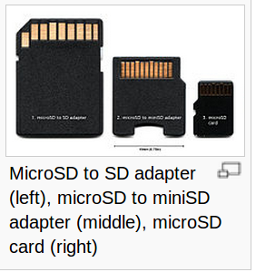
What is the SD/MMC?
Secure Digital縮寫SD,全名Secure Digital Memory Card,中文翻譯為安全數位卡,為一種記憶卡,被廣泛地於攜帶型裝置上使用,例如數位相機、個人數位助理和多媒體播放器等。SD卡的技術是建基於MMC(MultiMedia)卡格式上。SD卡有比較高的資料傳送速度,而且不斷更新標準。
SD 是一種 flash memory card 的標準,也就是一般常見的 SD 記憶卡,而 MMC 則是較早的一種記憶卡標準,目前已經被 SD 標準所取代.
後來還出了 SDHC(Secure Digital High Capacity),是由 SD 卡協會(SD Card Association)在 2006 年 3 月發表的 Secure Digital 高容量版本。SD 卡協會有强制規定,所有符合 SDHC 規範的設備都必須標明 “SDHC” 的標誌。
SDHC 與 SD 的主要差異在於,舊版本使用 FAT16 檔案系統,意思是管理檔案所在位置的表格用 16 位元表示,所以最多只能管理 65,536 個範圍,再考慮每個範圍能儲存 32KB 的資料量,所以 65536 × 32KB = 2GB,SD 卡容量上限只能到達 2GB。為解決 FAT16 格式可支援容量有限的問題,SDHC 改用了 FAT32 格式;依規格定義,容量最大可達到 32GB。
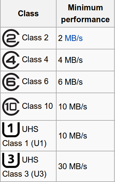
發佈 SDHC 的時候,制定了三種不同的級數 (Class),分別是 Class 2、Class 4 及 Class 6,表示該記憶卡穩定的最小存取速度。後來,又增加了 Class 10 及全新制定的 UHS(Ultra High Speed)標準。
What is the SDIO?
SDIO 是目前我們比較關心的技術,SDIO 顧名思義,就是 SD 的 I/O 介面(interface),不過這樣解釋可能還有點抽象。更具體的說明,SD 本來是記憶卡的標準,但是現在也可以把 SD 拿來插上一些週邊介面使用,這樣的技術便是 SDIO。
所以 SDIO 本身是一種相當單純的技術,透過 SD 的 I/O 接腳來連接外部週邊,並且透過 SD 上的 I/O 資料接位與這些週邊傳輸資料,而且 SD 協會會員也推出很完整的 SDIO stack 驅動程式,使得 SDIO 週邊(我們稱為 SDIO 卡)的開發與應用變得相當熱門。
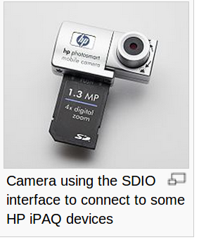
A SDIO (Secure Digital Input Output) card is an extension of the SD specification to cover I/O functions.
Host devices that support SDIO can use the SD slot to support:
- GPS receivers.
- digital cameras.
- RFID readers.
- FM radio tuners.
- TV tuners.
- Wi-Fi.
- Bluetooth.
Many other SDIO devices have been proposed, but it is now more common for I/O devices to connect using the USB interface.
SDIO cards support most of the memory commands of SD cards. SDIO cards can be structured as 8 logical cards, although currently, the typical way that an SDIO card uses this capability is to structure itself as one I/O card and one memory card.
SDIO bus topology
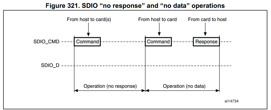
注意:若 Busy 信號被斷言 (SDIO_D0 pulled low),則 SDIO 並不會傳送任何資料
SDIO functional description
圖說明:
- SDIO_D0 預設是用來當作資料傳輸,而在初始化時,host 端可以設定其 data width。
- 當 MMC 連至 bus 時,MMC 可以支援只有 1-bit 模式。
- 當 SD/SD I/O 連至 bus 時,data transfer 可以由 host 端來設定是 SDIO_D0(1-bit mode) 或者是 SDIO_D3:0 而所有的 data lines 都是操作於 push-pull mode。
SDIO_CMD has two operational modes:
Open-drain for initialization (only for MMCV3.31 or previous)
Push-pull for command transfer (SD/SD I/O card MMC4.2 use push-pull drivers also for initialization)
SDIO_CK is the clock to the card:
- 在clock cycle 中 , 1 bit是用來切換command 或是 data lines.
- clock的頻率依照規格不同有所不同:
- between 0 and 20 MHz (for a MultiMediaCard v3.31).
- between 0 and 48 MHz (for a MultiMediaCard v4.0/4.2).
- between 0 and 25 MHz (for an SD/SD I/O card).
- The SDIO uses two clock signals:
- SDIO adapter clock(SDIOCLK = 48MHz is coming from a specific output of PLL (PLL48CLK) ).
- APB2 bus clock(PCLK2).
Frequency PCLK2 ≥ (3/8) * Frequency SDIO_CK
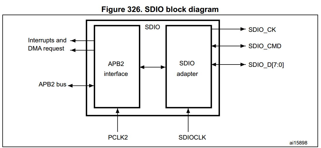
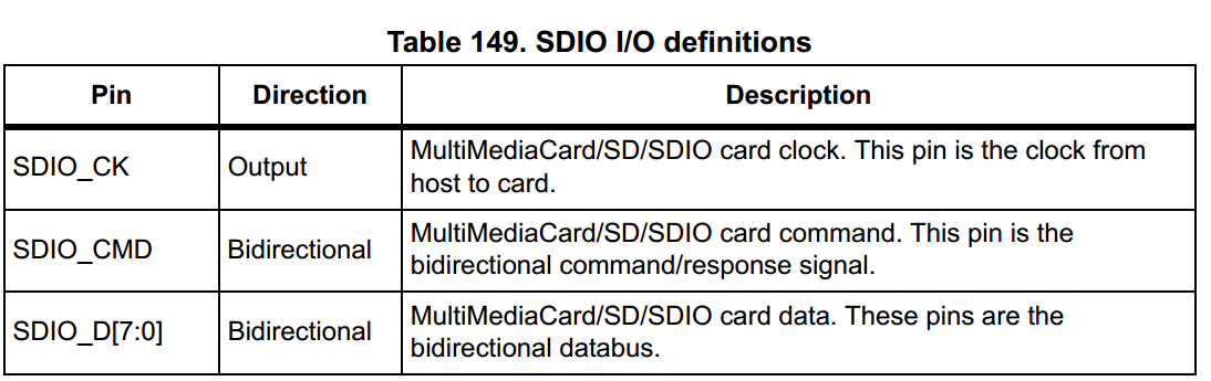
The signals shown in Table 149 are used on the MultiMediaCard/SD/SD I/O card bus
SDIO adapter
block diagram of an SDIO adapter.
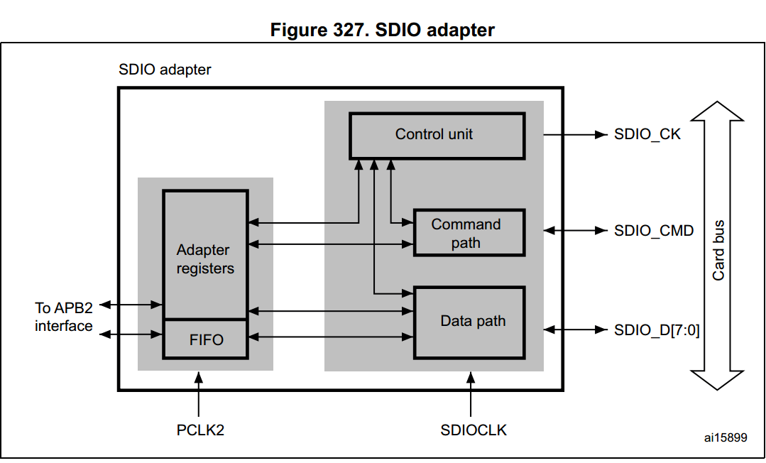
上圖中包含了五個子單元:
- Adapter register block
- Control unit
- Command path
- Data path
- Data FIFO
由圖中可以看出 , adapter registers 和 FIFO都是採用APB2 bus clock domain (PCLK2), 而control unit , command path , data path 則是採用SDIO adapter clock domain(SDIOCLK).
上圖中之左側部份(Adapter registers and FIFO): Adapter registers 主要包含了所有SDIO的暫存器 , 而這些暫存器是用來配置一些參數,以用來實現SD協定中的時序,最終目的是用來實現SD卡的命令傳輸。 而FIFO則是為了實現與data path的傳輸 , 而這兩個分別代表著對SD卡的兩種操作模式 , 一個是命令的傳輸 , 一個是資料的傳輸。
上圖中之右側 主要分為三個子單元,Control Unit, Command Path and Data Path。Control Unit 主要用來控制電源以及時鐘的控制,而這些控制是根據 Adapter registers 當中的暫存器來做配置,而 Command Path 連結SDIO_CMD,他用來控制命令的傳輸,最後 Data Path 則是連結 SDIO_D[7:0],控制資料的傳輸。底下將分單元描述各部零件。
Adapter register block
Adapter register block 包含了所有的 system registers。此外,adapter register block 亦會產生清除 multimedia card 中 static flag 的 signal。這種 clear signal 是根據在 SDIO Clear register 中對應的 bit location 是否為 1 而產生的。
Control Unit
這部份又在其內部分為兩個子單元,一個是 Power management,另一個是 Clock management,這兩個子單元都受 Adapter registers 控制。詳見下圖:
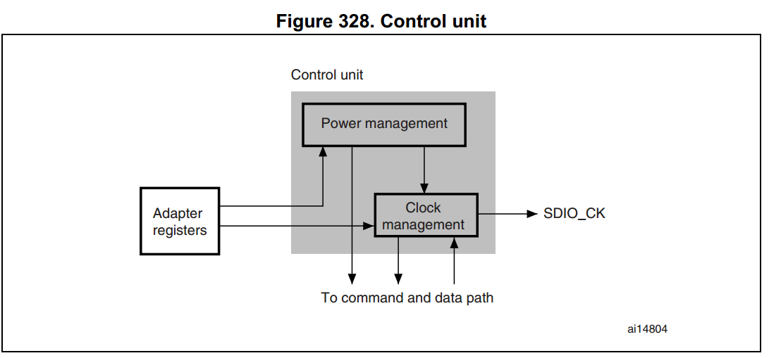
Power management
對 power 而言,會有三個時期:
- power-off
- power-up
- power-on
注意:若 power 處於 power-off 即 power-up 時期,power management subunit 就會停止 card bus 的 output signals。
Clock management
用來產生和控制 SDIO_CK,而其 SDIO_CK 又可選擇兩種模式:
- Clock Divide (SDIO_CK = SDIO_CLK/div)
- Clock Bypass (SDIO_CK = SDIO_CLK)
而在底下的情況下,Clock 是不輸出訊號的
- after reset
- 電源處於 power-off 或 power-up 時期
- 若省電模式被啟動且 card bus 處於 the
Idle狀態 (eight clock periods after both the command and data path subunits enter theIdlephase).
Command Path
Command path 用來傳遞外來命令與接收卡片回應,是 SDIO 中負責處理外部裝置 command 的單位。
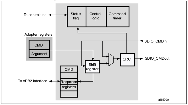
Command registers 中具有各 state flags 來表示 command path 目前的狀態,而狀態間的轉移可以用 state machine 表示:
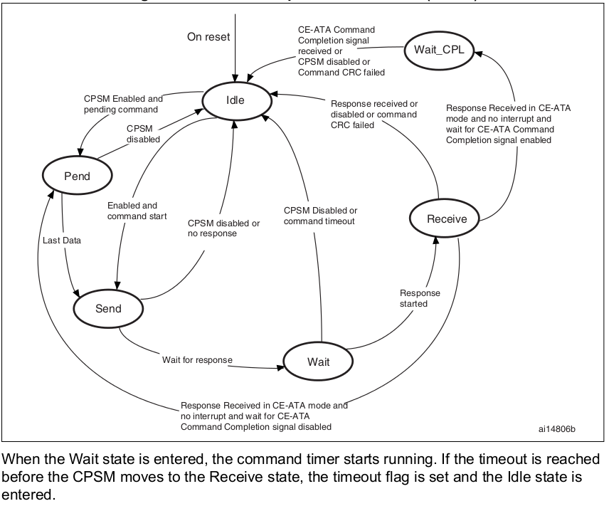
當 command register 被寫入且 enable bit 被設為真值,command 的傳送即告開始。Command 被傳送後,CPSM 會進入 Idle 狀態且自動設定 status flags 的值。若該命令需要回應,則等待回應。當回應產生後,command path 會比較回傳的 CRC 與內部產生的 code,然後對應的 status flag 會自動被設定。
注意:Command timeout 的值固定在 64 個 SDIO_CK。也就是在 Wait 狀態下,若 64 個 SDIO_CK 的時間過去後仍未收到回應,則 CPSM 將再次進入 Idle 狀態。
若 Interrupt bit 被設為真,command register 中的 timer 會被停用且 CPSM 開始等待 SD cards 發出的 interrupt request;若 Pending bit 被設為真,CPSM 進入 Pend 狀態,並等待自 data path 發送之 CmdPend signal;若偵測到 CmdPend signal,CPSM 進入 Send 狀態,此舉將讓 data counter 開始運作,並賦予其停止 command 的傳輸的驅動權。
注意:當 CPSM 每次進入 Idle 狀態時,會至少停留在此狀態 8 個 SDIO_CK 的時間,以滿足 N(CC) 與 N(RC) 的時間差限制。N(CC) 是兩個 host command 的最小延遲,N(RC) 則是 command 與 response 間的最小延遲。
底下則是典型 SDIO command transfer 的示意圖:
![]()
當 CPSM 不在 Send 狀態,SDIO_CMD 會處於 Hi-Z 狀態。
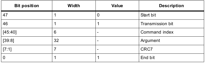
接著說明 command 與 response 的格式:
一般 Command(普通 MMC, SD card 與 SDIO 裝置)的長度固定在 48 個 bit,上面 CPSM 提到的 CE-ATA 則是 MMC v4.2 的延伸功能,其格式與普通 command 相同。Command path 是以半雙工模式運作,亦即同時間只能傳送 command 或接收 response。
Response 則分為 48 bit 的短回應與 136 bit 的長回應兩種,兩種都使用 CRC 作為錯誤檢測的依據。
注意:若 response 中未帶有 CRC,則外部裝置的驅動程式必須忽略 CRC failure 狀態。
底下是這兩種回應的詳細格式:
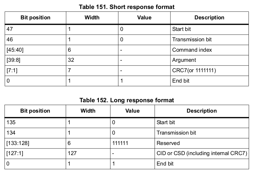
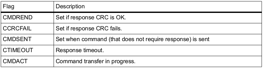
另外,在 command register 中存有 command index,這除了可以分辨 response 屬於哪種格式外(包含 6 個 bit 的資訊,Command Index in short format, [133:128] in long format),亦可分辨該 command 需不需要 response。Command path 並包含以下的 flag 指示目前的 command/response 傳輸狀態:
CRC chscksum 為 7 個 bit,在短格式中,以 CRC7 之前所有欄位的資料作計算;在長格式中,則以 CID/CSD 前 120 個 bit 為基準作計算(亦即不包含 start bit, transmission bit 與 6 個保留 bit)。
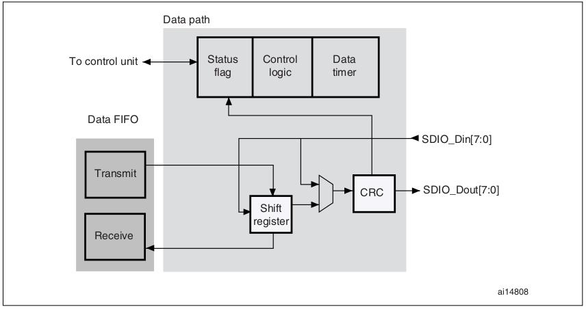
Data Path
Data path 負責資料的傳輸,底下是該子單元的 block diagram:
Data bus 的長度是可以透過 clock control register 控制的,若我們指定使用 4-bit 長的傳輸模式,則代表在每一個 clock cycle 中,會由 SDIO_D[3:0] 傳輸 4 bit 的資料;若為 8-bit 長,則為 SDIO_D[7:0];若 wide bus 模式未啟動,則單一 clock cycle 只傳輸一個 bit。
Data path 與 command path 相同,可以用 state machine 表示 data path 的各狀態間的關係與運作方式:
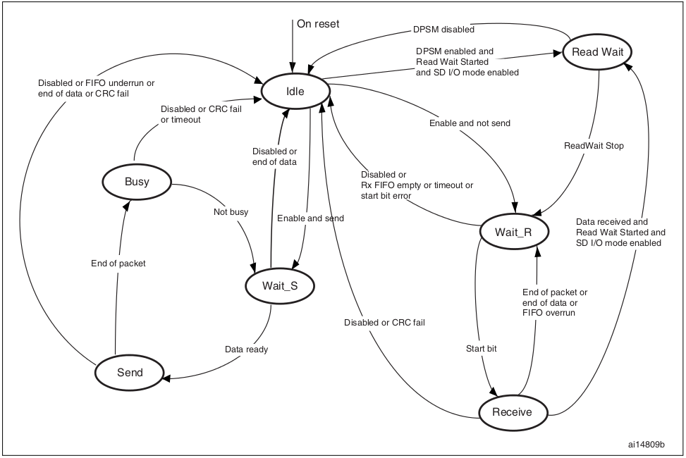
DPSM 運作在 SDIO_CK 的頻率上,包含若干狀態。
當 DPSM 啟動,會依據資料傳輸的方向,進入 Wait_S 或是 Wait_R 模式(Send and Receive)。
若在 Wait_S 狀態、且 transmit FIFO 中有 data,則DPSM 會移動至 Send 狀態,然後 data path 開始傳送資料至 card 中;若在 Wait_R 狀態、且收到 Start bit,則 DPSM 移動至 Receive 狀態,然後 data path 開始接受從 card 傳來的 data。
以下對各狀態進行解說:
Idle:data path 未活動,SDIO_D[7:0] 輸出 Hi-Z。當 data control register 被寫入且 enable bit 被設為真,DPSM 會載入 data counter 並寫入新值,且根據 data direction bit 來判斷要移動至
Wait_S狀態或Wait_R狀態。Wait_R:若 data counter 為零且 receive FIFO 為空時,DPSM 會移動至
Idle;若 data counter 不為零,DPSM 會等待來自SDIO_D的 start bit;若在 timeout 前收到 start bit,DPSM會移動至Receive狀態,然後自 block counter 讀取資料。若形成 timeout before 或者接收到錯誤的 start bit,DPSM 移動至Idle狀態且將 timeout status flag 設為真。Receive:自 card 接收的連續資料會寫至 data FIFO。根據 data control register 中的 transfer mode bit,我們可以知道 data transfer mode 是 block 或 stream:
– 若是 block mode,當 data block counter 達零時,DPSM 會一直等待直到收到 CRC。如果此 CRC 符合內部產生的 CRC,DPSM 移動至
Wait_R狀態;若無, CRC fail status flag 會被設為真且 DPSM 會移回Idle狀態。– 若是 stream mode,當 data counter 非零時 DPSM 會接收資料;若 data counter 為零,在 shift register 的剩餘資料會被寫入 data FIFO,然後 DPSM 移動至
Wait_R狀態。若發生 FIFO overrun error,DPSM 將 FIFO error flag 設為真然後移回Idle狀態。Wait_S:若 data block counter 為零時,DPSM 移動至
Idle狀態;若非,DPSM 會等待 data FIFO empty flag 被解除設定,然後移至Send狀態。Send:表示 DPSM 開始傳送資料至 card,根據 data control register 中的 transfer mode bit,我們可以知道 data transfer mode 是 block 或 stream:
– 若是 block mode,當 data block counter 達零時,DPSM 傳送內部產生的 CRC 與 end bit,然後移至
Busy狀態。– 若是 stream mode,且 enable bit 為高位及 data counter 非零時,DPSM 會傳送資料給 card,然後移至
Idle狀態。
若發生 FIFO underrun error,DPSM 將 FIFO error flag 設為高位且移動狀態至Idle。
Busy:DPSM 正在等待 CRC 的 status flag。
– 若 DPSM 沒收到 positive CRC status,它會移至
Idle狀態且設定 CRC fail status flag 為高位。– 若 DPSM 收到 positive CRC status、而且 SDIO_D0 不在低位 (the card is not busy) 時,它會移至
Wait_S狀態。
若 DPSM 在 Busy 狀態下發生 timeout,DPSM 會設定 data timeout flag 會移動至 Idle 狀態。若 DPSM 的狀態是 Wait_R 或 Busy 時,data timer 會被啟用,並產生 data timeout error:
- 當傳送 data 時,timeout 可能會發生在當 DPSM 停留在 ``Busy`` 狀態的時間超過了事先定義的 timeout 閾值。

- 當接收 data 時,timeout 可能會發生在當 DPSM 停留在 ``Wait_R`` 狀態的時間超過了事先定義的 timeout 閾值,且 data 結尾不為真時。
注意:為了符合 N(WR) 的時間間隔限制,DPSM 至少會停留在 Wait_S 兩個 clock period。N(WR) 是接收到來自 card 的回應與開始自 host 傳送資料此二動作間的 clock cycle 數
Data FIFO
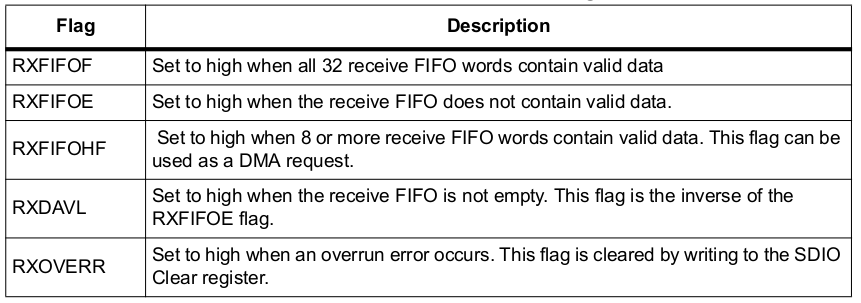
Data FIFO (first-in-first-out) 是 SDIO 中傳送/接收子單元的 data buffer。
FIFO 含有一 32-bit 寬與 32-word 深的 data buffer,以及一個傳送/接收邏輯電路。因為 data FIFO 運作在 APB2 的 clock domain (PCLK2),從所有在 SDIO clock domain (SDIOCLK) 運作的子元件接收的所有 signals 都會被 resynchronized。
根據 TXACT 與 RXACT 兩 flag 的狀態,FIFO 可以是被 disabled, transmit enabled, 或是 receive enabled。 TXACT 與 RXACT 相互排斥且被 data path 所驅動:
The transmit FIFO refers to the transmit logic and data buffer when
TXACTis assertedThe receive FIFO refers to the receive logic and data buffer when
RXACTis asserted
Transmit FIFO
Data can be written to the transmit FIFO through the APB2 interface when the SDIO is enabled for transmission.
The transmit FIFO is accessible via 32 sequential addresses. The transmit FIFO contains a data output register that holds the data word pointed to by the read pointer. When the data path subunit has loaded its shift register, it increments the read pointer and drives new data out.
If the transmit FIFO is disabled, all status flags are deasserted. The data path subunit asserts TXACT when it transmits data.
![]()
Receive FIFO
When the data path subunit receives a word of data, it drives the data on the write databus. The write pointer is incremented after the write operation completes. On the read side, the contents of the FIFO word pointed to by the current value of the read pointer is driven onto the read databus. If the receive FIFO is disabled, all status flags are deasserted, and the read and write pointers are reset. The data path subunit asserts RXACT when it receives data.
SDIO interrupt
- 當任何一個透過 mask register 預先選擇的特定 flags 之 status flag 為 high 時,interrupt logic 將會產生一個 interrupt request。又若某個 mask
flag 被 set 的話,其對應的 status flag 也會產生 interrupt request。
Sample Code
https://github.com/JackABK/STM32F4-FreeRTOS/tree/master (Switch master branch)
Initialization
.. code-block:: prettyprint
SD_Error SD_Init(void) { __IO SD_Error errorstatus = SD_OK;
/* SDIO Peripheral Low Level Init */
SD_LowLevel_Init();

//SDIO_DeInit();

errorstatus = SD_PowerON();

if (errorstatus != SD_OK)
{
  /*!< CMD Response TimeOut (wait for CMDSENT flag) */
  return(errorstatus);
}

errorstatus = SD_InitializeCards();

if (errorstatus != SD_OK)
{
  /*!< CMD Response TimeOut (wait for CMDSENT flag) */
  return(errorstatus);
}

/*!< Configure the SDIO peripheral */
/*!< SDIO_CK = SDIOCLK / (SDIO_TRANSFER_CLK_DIV + 2) */
/*!< on STM32F4xx devices, SDIOCLK is fixed to 48MHz */
SDIO_InitStructure.SDIO_ClockDiv = SDIO_TRANSFER_CLK_DIV;
SDIO_InitStructure.SDIO_ClockEdge = SDIO_ClockEdge_Rising;
SDIO_InitStructure.SDIO_ClockBypass = SDIO_ClockBypass_Disable;
SDIO_InitStructure.SDIO_ClockPowerSave = SDIO_ClockPowerSave_Disable;
SDIO_InitStructure.SDIO_BusWide = SDIO_BusWide_1b;
SDIO_InitStructure.SDIO_HardwareFlowControl = SDIO_HardwareFlowControl_Disable;
SDIO_Init(&SDIO_InitStructure);

/*----------------- Read CSD/CID MSD registers ------------------*/
errorstatus = SD_GetCardInfo(&SDCardInfo);

if (errorstatus == SD_OK)
{
  /* Select Card*/
  errorstatus = SD_SelectDeselect((uint32_t) (SDCardInfo.RCA << 16));
}

if (errorstatus == SD_OK)
{
  errorstatus = SD_EnableWideBusOperation(SDIO_BusWide_4b);
}

return(errorstatus);
}
- media_read
.. code-block:: prettyprint
int media_read(unsigned long sector, unsigned char *buffer, unsigned long sector_count)
{
    unsigned long i;
    SD_Error error;
    for (i=0;i<sector_count;i++)
    {
        // ...
        // Add platform specific sector (512 bytes) read code here
        // ...

        while(SD_GetStatus()!=SD_TRANSFER_OK);
        error=SD_ReadBlock(buffer,sector*512,512);
        while(SD_GetStatus()!=SD_TRANSFER_OK);
        sector ++;
        buffer += 512;
    }

    return 1;
}- media_write
.. code-block:: prettyprint
int media_write(unsigned long sector, unsigned char *buffer, unsigned long sector_count)
{
    unsigned long i;
    SD_Error error;

    for (i=0;i<sector_count;i++)
    {
        // ...
        // Add platform specific sector (512 bytes) write code here
        // ...
        while(SD_GetStatus()!=SD_TRANSFER_OK);
        error=SD_WriteBlock(buffer,sector*512,512);
        while(SD_GetStatus()!=SD_TRANSFER_OK);
        sector ++;
        buffer += 512;
    }

    return 1;
}- FatFs
.. code-block:: prettyprint
void example_fat_fs()
{
    FL_FILE *file;

    // Initialise media
    media_init();

    // Initialise File IO Library
    fl_init();

    // Attach media access functions to library
    if (fl_attach_media(media_read, media_write) != FAT_INIT_OK)
    {
        printf("ERROR: Media attach failed\n");
        return;
    }

    // List root directory
    fl_listdirectory("/");

    // Create File
    file = fl_fopen("/file.bin", "w");
    if (file)
    {
        // Write some data
        unsigned char data[] = { 1, 2, 3, 4 };
        if (fl_fwrite(data, 1, sizeof(data), file) != sizeof(data))
            printf("ERROR: Write file failed\n");
    }
    else
        printf("ERROR: Create file failed\n");

    // Close file
    fl_fclose(file);

   // Delete File
   // if (fl_remove("/file.bin") < 0)
   // printf("ERROR: Delete file failed\n");

    // List root directory
    fl_listdirectory("/");

    fl_shutdown();
}
Demo
- https://www.youtube.com/watch?v=go-L5ERTrso
