版本 72aa9a20b6139af79f2200ff09338d91db6b990d
Changes from 72aa9a20b6139af79f2200ff09338d91db6b990d to current
---
title: General-purpose Input/Output (GPIO)
categories: GPIO, STM32F4
title: General Purpose Input/Output (GPIO)
categories: ARM, STM32, STM32F4, STM32F429, GPIO, Peripheral
...
Introduction
============
**General Purpose Input/Output (GPIO)** is a generic pin on a chip whose behavior (including whether it is an input or output pin) can be controlled (programmed) by the user at run time.
Introduction - 簡介
===================
**General Purpose Input/Output (GPIO)**
a generic pin on an integrated circuit whose behavior, including whether it is an input or output pin, can be controlled by the user at run time.
通常我們program使用的data都是放在memory比較多,而GPIO也提供類似的操作方法給programmer(讓我們去更改記憶體內容就可以去控制pin,並影響周遭設備的運行),但真正的設備的位置並非真正落在記憶體上(如:LED、Button、...等),故GPIO的核心是記憶體操作與設備之間的一些電路特性。
* GPIO 是種具有彈性且可以藉由軟體控制 (software-controlled) 的數位訊號
* 常見於開發版邊緣, 以針腳 (Pin) 的形式呈現
- 這些針腳即是開發版與外界溝通的重要橋樑
- 簡單例子, 想像成是開關, 使用者可以打開或關閉 (input), 或由開發版來打開或關閉 (output)
Main Feature
============
GPIO雖然建立起記憶體與設備之間的橋梁,但也並非我們就可以隨意使用,我們必須要經過設定之後才能讓我們想要的設備正常工作。
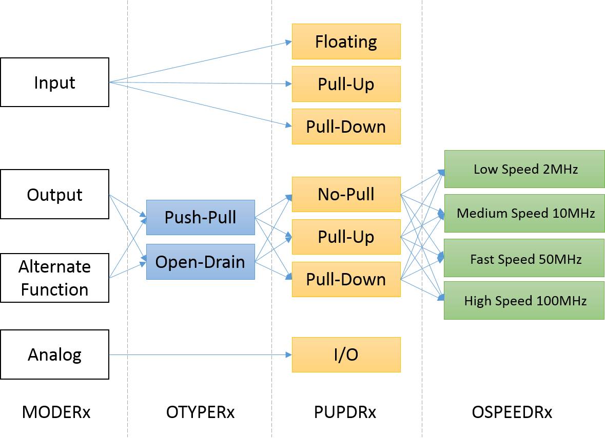
* 每個 GPIO 可以被當成 input, output, analog 或 alternate function
- alternate function 是指其他的的功能, 如 I2C, SPI, USART, CCP, PWM, Clock 等。如何控制則取決於外部設備 (peripheral)
一個pin通常可被設定成input、output、alternate function或analog,input會有兩種狀態表現(floating, pull-up/down),output也有兩種狀態表現(push-pull with pull-up/pull-down or open drain with pull-up/down)。
STM32F4xx GPIO特性
=====================================
- input/output方向解說 : input是指記憶體方接收來自設備的訊號源,output是指記憶體傳送訊號給設備。
* 所有 GPIO 具有容許較高的電流能力與四種速度選擇,根據不同設定管理雜訊、電耗與電磁波
* 最大 I/O 切換速度可以支援到 90 MHz
* STM32F4xx 每個 GPIO Port 有 10 個 32-bit 暫存器 (Register)
- Configuration Register: GPIOx_MODER, GPIOx_OTYPER, GPIOx_OSPEEDR 與 GPIOx_PUPDR
- Data Register: GPIOx_IDR and GPIOx_ODR
- Set/Reset Register: GPIOx_BSRR
- Locking Register: GPIOx_LCKR 【防止因錯誤而改變GPIO的用途(accidental repurposing)】
- Alternate Function Selection Register: GPIOx_AFRH 與 GPIOx_AFRL
當pin被設定成input時,非analog的設定下,我們可以利用GPIO的input data register(GPIOx_IDR) 或是memory中提供給目標設備的data register (當設成alternate function的時候)去接收data。
一個pin通常可被設定成input、output、alternate function或analog, (alternate function和analog只有在特定腳位)
當pin被設定成output時,非analog的設定下,GPIO本身有提供output data register (GPIOx_ODR)來對目標設備做控制,但要是pin不是使用原本預先定義好的功能時(非預先定義的功能都算是alternate function的類別),此時要用memory中,另外規劃給目標設備用的register。
input會有兩種狀態(floating, pull-up/down),output也有兩種狀態(push-pull, open drain with pull-up/down resistors)。
如果pin被設成analog的話,無論input or output都會由adc那邊做處理。
**input/output方向 : input是指記憶體方接收來自設備的訊號源,output是指記憶體傳送訊號給設備。**
Functional Description
======================
各模式下的操作方式:
- Input mode:我們可以利用GPIO的input data register(GPIOx_IDR) 或是memory中提供給目標設備的data register (當設成alternate function的時候)去接收data。
- Output mode(非analog):GPIO提供output data register (GPIOx_ODR)及Bit set/reset register (GPIOx_BSRR)來對目標設備做控制
- Alternate function:此時要用memory中另外規劃給目標設備用的register對Pin腳進行控制。
- Analog mode:input和output會轉由adc/dac那邊做處理。
Functional Description - 功能敘述
================================
input
-------------------
- floating vs. pull-up/pull-down
當input pin被處在高阻抗的模式下,若沒有外部訊號源進來的話,此時是無法確定pin的狀態(不能確定現在處在高電位或低電位),除非有外部訊號來驅動電路。換句話說,input floating,這個input電位狀態完全是由外部訊號來決定,沒有訊號驅動的話,就會呈現高阻抗狀態。
剛剛提到floating在沒有外部訊號驅動的情況下是呈現高阻抗狀態(無法確定電位狀態=>不能明確表示現在值是0或1),如果我們需要這個pin有一個明確的預設狀態時,必須借助pull-up(pull-down)resistor來做調整,在pull-up resistor(pull-up外接高電壓,pull-down通常會接地)加入之下,讓pin的維持在明確的高電壓狀態(pull-down則是讓pin維持在低電壓狀態)。舉例來說,如果我們定電壓在3-4 V之間是1的狀態,0-1之間是0的狀態,高阻抗的時候,電壓是不明確的,有可能電壓值會落在1-3之間的不明確地帶,甚至是沒有在任何一個狀態維持一段時間,此時的狀態是未定的,但如果我們加入pull-up resistor的話,這個pin接受來自pull-up另一端的電壓供應,讓pin至少維持在3v以上時,我們就可以確定在沒有外部訊號驅動時,pin是維持在高電位狀態。
pull-up/pull-down電阻在大部分腳位上為40kΩ,在PA10/PB12上為10kΩ。至於其範圍,可以參考Datasheet p.110,Table 47. I/O static characteristics。
--------
- 施密特觸發器(Schmitt trigger)
將類比訊號的波形整成數位電路所能處理的方波波形,以利被input register讀取(處理完只能分辨出高低電位的差別)。
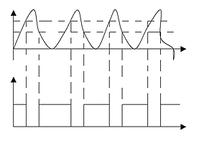
(施密特觸發器具有整流效果)
output
-------------------
- push-pull with pull-up/pull-down
- open-drain with pull-up/pull-down
- push-pull vs open-drain mode
output處在push-pull模式下時,當output registers為"0"時輸出低電位,"1"時輸出高電位。而在open-drain模式下,"0"輸出低電位,"1"時為高阻抗(Z)狀態,電位無法確定。此兩種模式下,pin皆可pull-up/pull-down。
當有多個輸出pin在互相連通時(例如一個bus),若有兩個輸出呈不同狀態,電路上的電位便無法確定。因此,除了正在輸出的pin以外,其他pin應在高阻抗態以免干擾。以bus的例子來說,若令所有pin皆在open-drain mode pull-up,並使非輸出端pin為"1"(Z),當輸出pin為"1"時,bus為高電位(因為pull-up);當輸出pin為"0"時,bus為低電位。
analog
-------------------
前面所述的input/output跟現在要談的類比模式是不一樣的類型,前者的資料型態主要是高低電位的數位型態(0/1的分別),而類比訊號是普遍自然界的訊號型態,故當我們設定成類比輸入的模式時,進來GPIO pin的原始訊號源在還沒經過施密特觸發器(Schmitt trigger)會有另一個線路將訊號做導向(通常是要導到ADC去),另一方面,當我們用了類比輸出模式後,GPIO的內部將會有一條線路接收DAC處理完的類比訊號,在經過此pin傳遞到外部去。
- 施密特觸發器(Schmitt trigger) : 將類比訊號的波形整成數位電路所能處理的方波波形(處理完只能分辨出高低電位的差別)。
.. image:: /embedded/Schmitt_trigger.jpg
(施密特觸發器具有整流效果)
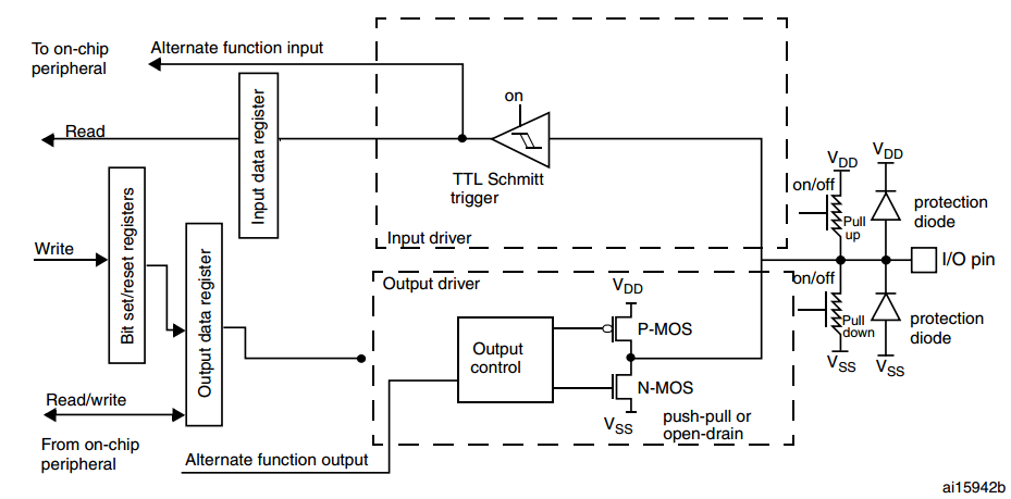
basic structure (P.137, **Figure 13. Basic structure of a five-volt tolerant I/O port bit** in Reference manual)
basic structure (P.266, **Figure 25. Basic structure of a five-volt tolerant I/O port bit** in Reference manual)
-------------------------------------------------------------------------------------------------------------------
.. image:: /embedded/GPIO_basic_src.PNG
- VDD:芯片內部的工作電壓
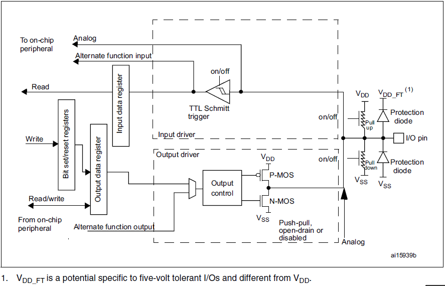
- VDD:晶片內部的工作電壓
- VDD_FT : I/O port專用電壓,與VDD不同
- VSS:接地點
- protection diode : 防止輸入電壓超過一定範圍。當電壓低於VSS時,電流通過protection diode流入pin;當電壓高於VDD_FT時,電流流出pin。
Configuration
=============
Input configuration (P.143, **6.3.9 Input configuration** in Reference manual)
補充: TTL vs CMOS
- TTL由電阻器和三極體而組成,CMOS內部零件多以金屬氧化物半導體組成。
- 就早期而言,TTL的速度較CMOS快,但功耗較高。但近年來CMOS在速度方面已經超越TTL。
- TTL懸空一般會呈高電位,CMOS則為不定態。
Configuration - 配置圖
=======================
Input configuration (P.273, **8.3.9 Input configuration** in Reference manual)
------------------------------------------------------------------------------
.. image:: /GPIO_ Input_configurations.png
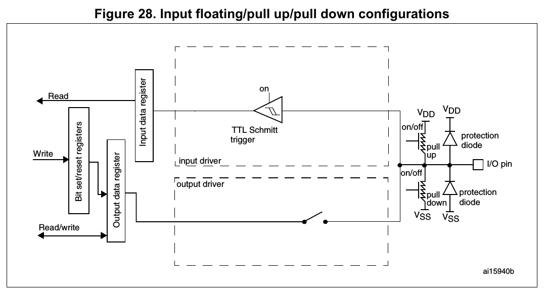
When the I/O port is programmed as Input:
- the output buffer is disabled
- the Schmitt trigger input is activated
- 這種模式處理的數位訊號只在意高低電位的差別(開關控制)。
- 這種模式處理的數位訊號只在意高低電位的差別(開關控制)。
- the pull-up and pull-down resistors are activated depending on the value in the GPIOx_PUPDR register
- 想要讓pin的state變成一個確定的狀態,可以設定pull-up/pull-down的使用。
- 想要讓pin的state變成一個確定的狀態,可以設定pull-up/pull-down的使用。
- The data present on the I/O pin are sampled into the input data register every AHB1 clock cycle
- input data的更新主要就是以AHB1本身的更新週期做決定,每一個cycle抵達時,data register就會根據當時Schmitt trigger整流完的狀態做更新。
- input data的更新主要就是以AHB1本身的更新週期做決定,每一個cycle抵達時,data register就會根據當時Schmitt trigger整流完的狀態做更新。
- A read access to the input data register provides the I/O State
- 對data register的理解,我覺得用'狀態'比'數值'的敘述來的更好(大部分都是開關,就是外部訊號源是否有狀態改變,如 : button的按下與放開),而此處寫I/O state的意思是,即使我們現在是設成output(如 : LED控制),但我們仍然可用input data register來檢查LED現在的狀態。
- 對data register的理解,我覺得用'狀態'比'數值'的敘述來的更好(大部分都是開關,就是外部訊號源是否有狀態改變,如 : button的按下與放開),而此處寫I/O state的意思是,即使我們現在是設成output(如 : LED控制),但我們仍然可用input data register來檢查LED現在的狀態。
Output configuration (P.144, **6.3.10 Output configuration** in Reference manual)
Output configuration (P.274, **8.3.10 Output configuration** in Reference manual)
---------------------------------------------------------------------------------
.. image:: /GPIO_ Output_configurations.png
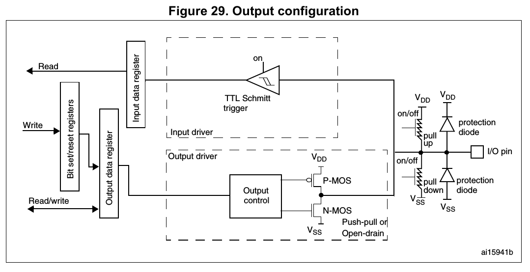
When the I/O port is programmed as output:
.. TODO: Output Control
- The output buffer is enabled:
- Open drain mode: A “0” in the Output register activates the N-MOS whereas a “1” in the Output register leaves the port in Hi-Z (the P-MOS is never activated)
- Push-pull mode: A “0” in the Output register activates the N-MOS whereas a “1” in the Output register activates the P-MOS
- Open drain mode: A “0” in the Output register activates the N-MOS whereas a “1” in the Output register leaves the port in Hi-Z (the P-MOS is never activated)
- Push-pull mode: A “0” in the Output register activates the N-MOS whereas a “1” in the Output register activates the P-MOS
- 如前所述,設定Open drain / Push-pull的使用。
- The Schmitt trigger input is activated
- The weak pull-up and pull-down resistors are activated or not depending on the value in the GPIOx_PUPDR register
- The data present on the I/O pin are sampled into the input data register every AHB1 clock cycle
- A read access to the input data register gets the I/O state
- A read access to the output data register gets the last written value
- 不一定與當下pin的狀態相同
Alternate function configuration (P.144, **6.3.11 Alternate function configuration** in Reference manual)
Alternate function configuration (P.275, **8.3.11 Alternate function configuration** in Reference manual)
---------------------------------------------------------------------------------------------------------
.. image:: /GPIO_Alternate_function_configuration.PNG
When the I/O port is programmed as alternate function:
- The output buffer can be configured as open-drain or push-pull
- The output buffer is driven by the signal coming from the peripheral (transmitter enable and data)
- The Schmitt trigger input is activated
- The weak pull-up and pull-down resistors are activated or not depending on the value in the GPIOx_PUPDR register
- The data present on the I/O pin are sampled into the input data register every AHB1 clock cycle
- A read access to the input data register gets the I/O state
Remark:
GPIOx_AFRL[31:0] and GPIOx_AFRH[31:0] provide ways to select alternation functions. However, different alternate functions maps to different bits of ports. Table below is part of alternate function mapping, which is mainly about USART2/3.
For more information, please refer to **Table 9. Alternate function mapping** from P.60-68 in STM32F407xx Datasheet.
.. image:: /embedded/af_mapping.png
GPIOx_AFRL[31:0] and GPIOx_AFRH[31:0] provide ways to select alternation functions. However, different alternate functions maps to different bits of ports.
For more information, please refer to **Table 12. Alternate function mapping** from P.73 in STM32F429xx Datasheet.
Analog configuration (P.145, **6.3.12 Analog configuration** in Reference manual)
Analog configuration (P.276, **8.3.12 Analog configuration** in Reference manual)
---------------------------------------------------------------------------------
.. image:: /GPIO_Analog_configurations.PNG
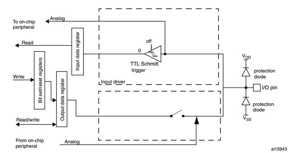
When the I/O port is programmed as analog configuration:
- The output buffer is disabled
- The Schmitt trigger input is deactivated, providing zero consumption for every analog value of the I/O pin. The output of the Schmitt trigger is forced to a constant value (0).
- The weak pull-up and pull-down resistors are disabled
- Read access to the input data register gets the value “0”
Note: In the analog configuration, the I/O pins cannot be 5 Volt tolerant.
- analog operating voltage (VDDA) max at 3.6V
Demo
====
工具介紹
-------
.. image:: /embedded/BNC line.JPG
[**Note2: Sampling jitter**](http://en.wikipedia.org/wiki/Jitter)
- BNC對鱷魚夾線
In analog to digital and digital to analog conversion of signals, the sampling is normally assumed to be periodic with a fixed period—the time between every two samples is the same. If there is jitter present on the clock signal to the analog-to-digital converter or a digital-to-analog converter, the time between samples varies and instantaneous signal error arises.
.. image:: /embedded/oscilloscope.JPG
- 示波器(oscilloscope) 畫面很差...
示波器驗證
Registers - 暫存器
==================
Overview
---------
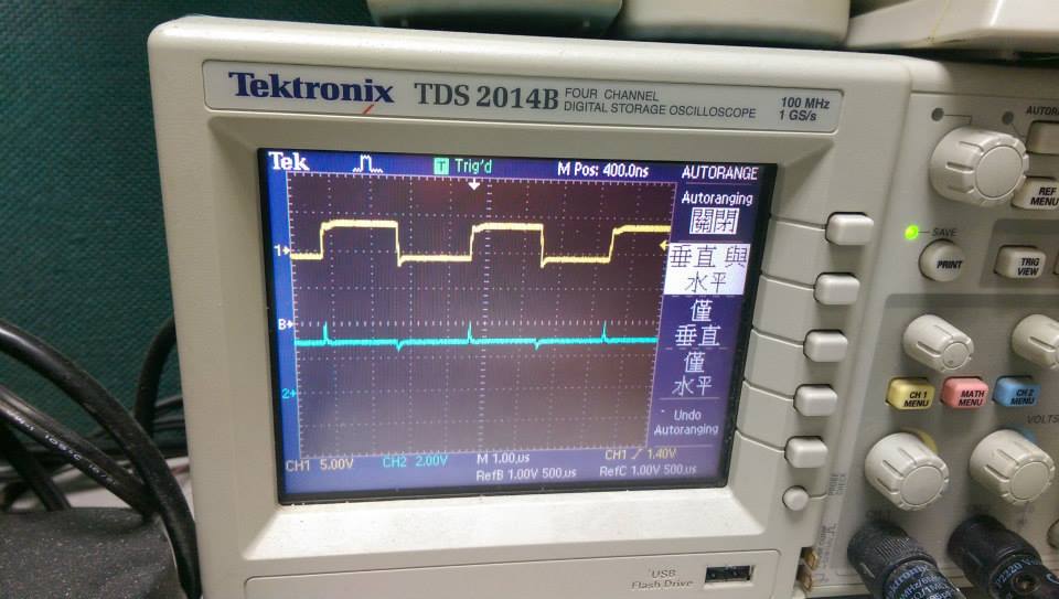
.. image:: /embedded/stable.JPG
- Mode, Speed, Type, PuPd 對應表
- 示波器我們調整的scale是1 volt為單位。
- 我們接線是使用BNC對鱷魚夾線,黑接Groud,紅接要觀察的Pin。此圖為我們還沒做任何操作呈現的狀態。
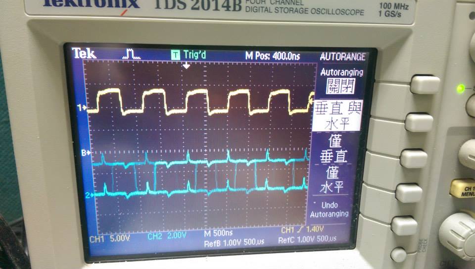
.. image:: /embedded/button_pressed.JPG
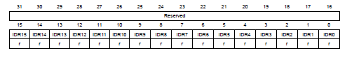
P.278, **GPIO port mode register (GPIOx_MODER)** in Reference manual
--------------------------------------------------------------------------
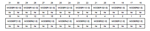
MODERy[1:0]決定第y pin GPIO使用的configuration,2個bit為一組
- 以button做為觀察GPIO input的部份
- USER button對應的腳位為PA0
- 按下button馬上放開後會產生一個小方波,由此可知,按下button是產生高電位訊號。(看'按下'多久高電位就維持多久)
- 00: Input
- 01: output mode
- 10: Alternate function mode
- 11: Analog mode
- 當reset後,GPIOA_MODER=0xA800 0000、GPIOB_MODER=0x0000 0280,其他皆為0。
* PA3, PA4, PB13, PB14, PB15 為 Debug Pin in AF
.. image:: /embedded/LEDOn_2.8v.JPG
P.279, **GPIO port output type register(GPIOx_OTYPER)** in Reference manual
---------------------------------------------------------------------------
決定在output時使用的模式(如前面Functional Description.output所述)。
- 用LED4來觀察GPIO output的部份
- LED4對應的腳位是PD12,當LED4亮的時候,我們可以看到波形產生變化(從0v左右的位置升到高電位2.8v左右)
- 0: Output push-pull
- 1: Output open-drain
- reset皆為0x0000 0000
.. image:: /embedded/PD12_PD14CNT.JPG
P.279, **GPIO port output speed register (GPIOx_OSPEEDR)** in Reference manual
------------------------------------------------------------------------------
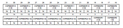
OSPEEDRy[1:0]決定output的速度。在不同的電容與電壓(VDD)下,輸出頻率可能不同,以下只列出代表值。
- 我們在接Pin的過程的時候,發現有些燈會亮起來,圖中紅色鱷魚夾線把PD12跟PD14同時夾起來,LED5在LED4亮起來的時候也會亮,對照PD14的位置是LED5。
- 我們觀察示波器用的Code只有對button跟LED4做設定,我們推測原因是LED4亮起來的時候,PD12處於高電位狀態,而鱷魚夾線連通PD14讓此腳位也處於高電位使LED5也亮起來了。
- 00: Low speed (2MHz)
- 01: Medium speed (10MHz)
- 10: Fast speed (50MHz)
- 11: High speed (100MHz)
- reset GPIOB_OSPEEDR=0x0000 00C0,其他皆為皆為0x0000 0000
- 速度越高,雜訊與耗電量越多。
- 在其他狀態下的速度,可以參考 datasheet p134 table 58. I/O AC Characteristics
Code Section
-------------
* 雜訊的來源
- Thermal noise
在電阻性的材料中,由於熱擾動的影響,造成材料內電子或電
洞等電荷載體產生隨機的速度擾動,這種類似布朗運動
- Shot noise
散粒雜訊通常存在于真空管中或半導體內,這種電子由負極到正極經外部電路的隨機運動
當電壓超過一定的臨界值而電流流出呈現散亂的形狀
sample code download :
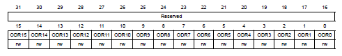
P.280, **GPIO port pull-up/pull-down register (GPIOx_PUPDR)** in Reference manual
---------------------------------------------------------------------------------
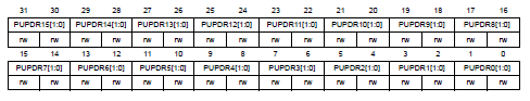
PUPDRy[1:0]決定pin y是否pull-up/pull-down
.. code-block:: c
- 00: No pull-up, pull-down
- 01: Pull-up
- 10: Pull-down
- 11: Reserved
- reset GPIOA_PUPDR=0x6400 0000、GPIOB_PUPDR=0x0000 0100,其他0x0000 0000。
git clone https://github.com/shengwen1997/stm32_GPIO_demo.git
cd stm32_GPIO_demo/
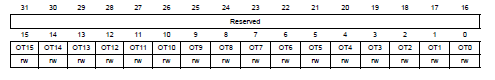
P.280, **GPIO port input data register (GPIOx_IDR)** in Reference manual
------------------------------------------------------------------------
讀取IDRy為input y的值。
test for code :
- Bits 31:16 Reserved, must be kept at reset value.
- Bits 15:0 IDRy: Port y input data
- register為read-only & word mode access only
- Reset: 0x0000 XXXX (X=undefined)
.. code-block:: c
P.281, **GPIO port output data register (GPIOx_ODR)** in Reference manual
-------------------------------------------------------------------------
輸出pin output的值。
make
make flash
- Bits 31:16 Reserved, must be kept at reset value.
- Bits 15:0 ODRy: Port output data
- Reset: 0x0000 0000
測試方法 :
P.281, **GPIO port bit set/reset register (GPIOx_BSRR)** in Reference manual
----------------------------------------------------------------------------
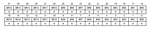
set或reset對應pin output data register的值。
- input使用button作為範例,output是LED控制。
- Bits 31:16 BRy: reset bit y
- Bits 15:0 BSy: set bit y
- 0: no action ,1:set/reset
- write-only ,讀取會得到0
- Reset: 0x0000 0000
stm32f4_discovery library的預先定義(in libstm/Utilities/STM32F4-Discovery/stm32f4_discovery.h) :
P.281, **GPIO port configuration lock register (GPIOx_LCKR)** in Reference manual
---------------------------------------------------------------------------------
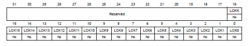
若給bit 16(LCKK)一個正確的write sequence,可以鎖住bits [15:0]對應的configurations。
當lock sequence正確執行之後,GPIOx_LCKR在下次reset之前無法修改。
.. code-block:: c
- Bit 16 LCKK[16]: Lock key
- 0: Port configuration lock key not active
- 1: Port configuration lock key active
- 只能在lock sequence時寫入
- Bits 15:0 LCKy: lock bit y
- 0: Port configuration not locked
- 1: Port configuration locked
- Lock sequences pseudocode
#define LEDn 4
```c
WR LCKR[16] = ‘1’ + LCKR[15:0]
WR LCKR[16] = ‘0’ + LCKR[15:0]
WR LCKR[16] = ‘1’ + LCKR[15:0]
RD LCKR
RD LCKR[16] = ‘1’ (optional, confirm only)
```
#define LED4_PIN GPIO_Pin_12
#define LED4_GPIO_PORT GPIOD
#define LED4_GPIO_CLK RCC_AHB1Periph_GPIOD
#define LED3_PIN GPIO_Pin_13
#define LED3_GPIO_PORT GPIOD
#define LED3_GPIO_CLK RCC_AHB1Periph_GPIOD
- Lock sequences in c lib ( `STM32F4xx_StdPeriph_Driver/src/stm32f4xx_gpio.c` : `void GPIO_PinLockConfig()` )
```c
tmp |= GPIO_Pin;
/* Set LCKK bit */
GPIOx->LCKR = tmp;
/* Reset LCKK bit */
GPIOx->LCKR = GPIO_Pin;
/* Set LCKK bit */
GPIOx->LCKR = tmp;
/* Read LCKK bit*/
tmp = GPIOx->LCKR;
/* Read LCKK bit*/
tmp = GPIOx->LCKR;
```
在執行中,LCK[15:0]的值不可改變,否則lock失敗。
P.283, **GPIO alternate function low/high register(GPIOx_AFRL/GPIOx_AFRH)** in Reference manual
-----------------------------------------------------------------------------------------------

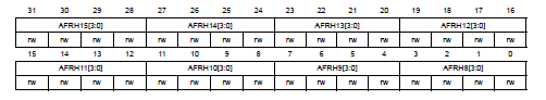
選擇pin y的alternate function。
- AFRLy/AFRHy : Alternate function selection for bit y
- AFRLy/AFRHy = 0000~1111 分別對應AF0~AF15
參考 Datasheet p.73~83 對照表,一個Pin可以對應一個alternate function
Demo - 測試實驗
==============
實驗設備
--------
* 除了STM32本身外,我們使用一台訊號產生器與一台示波器。
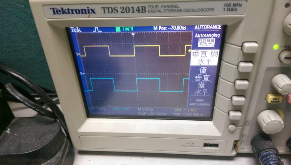
* 將訊號產生器輸出(+)接到示波器的channel 1(黃色)與 PG9,STM32的輸出PG13接示波器的channel 2(藍色)
- demo3, demo4
* 訊號產生器的接地(-)接到STM32的GND與示波器channel 1/2的負極。
--------
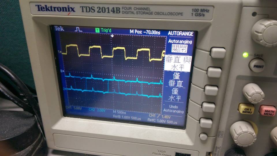
* 90.9Hz ,方波
* 起始狀態,程式將 PG9 的輸入 GPIOA_IDR shift 後送到 GPIOG_ODR,由 PG13 輸出。
- demo3, demo4
--------
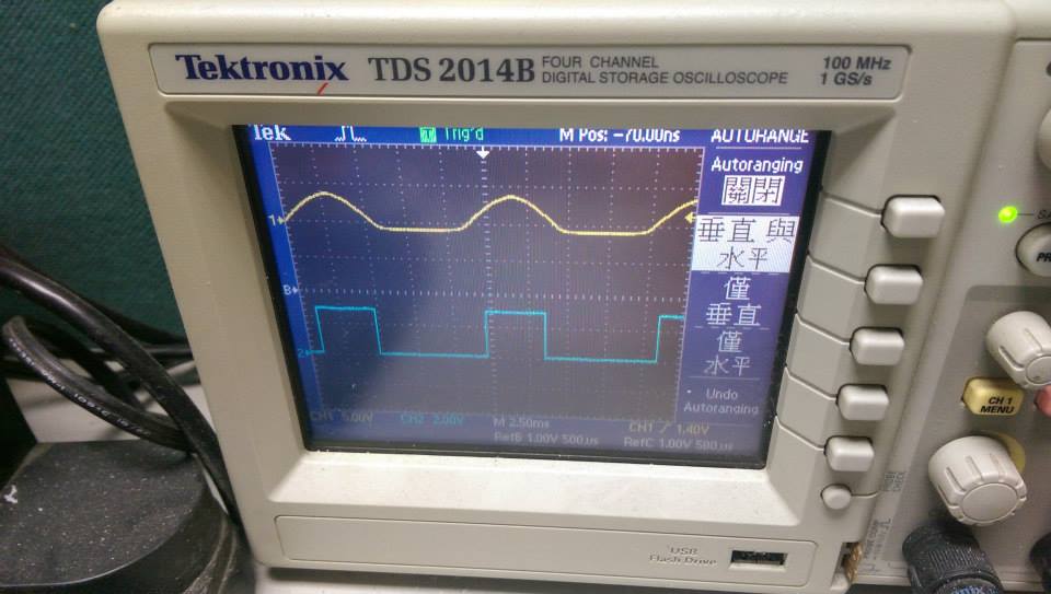
* 90.9Hz ,sin波
--------
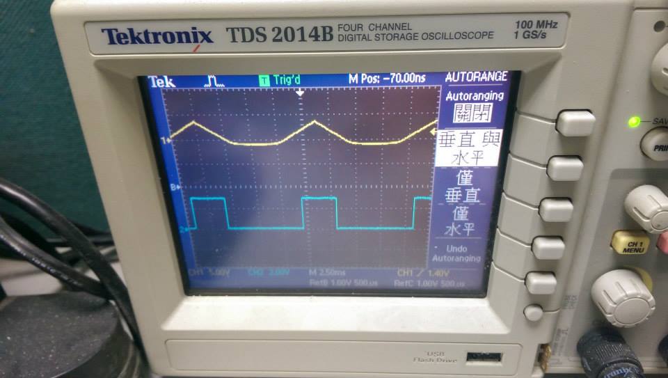
* 90.9Hz ,三角波
--------
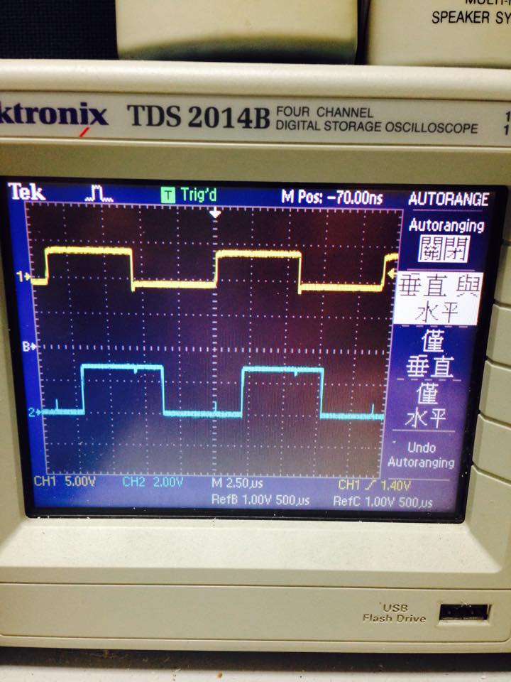
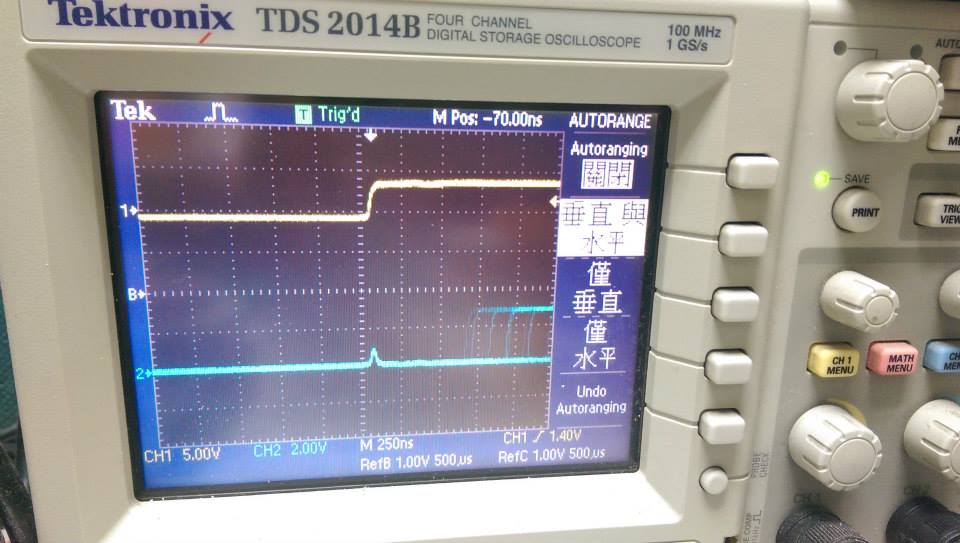
* 87000HZ ,interrupt with function call
* visible interrupt delay ,about 2000ns
- demo4 使用 GPIO_ToggleBits 切換
--------
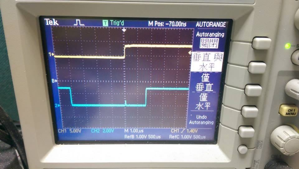
* 833000Hz ,interrupt with function call
* 頻率再增加, 會造成無法正常的解析波形
--------
* polling with function call
* 使用polling的結果,delay大約750ns
- demo3 使用 GPIO_ToggleBits 切換
- 與 demo4 相比會波型會抖動
--------
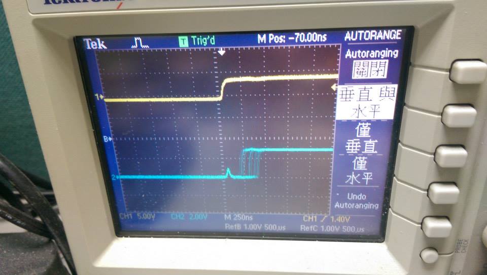
* 88500Hz ,interrupt without function call
* interrupt不用function call,delay大約1500ns
- demo4 使用 GPIOG->ODR = GPIOA->IDR << 13; 切換
--------
* polling without function call
* 不用function call,delay大約250ns
- demo3 使用 GPIOG->ODR = GPIOA->IDR << 13; 切換
--------
* 260000Hz ,interrupt without function call
* 頻率加快的結果
- demo4
- 波型呈現連續都是高電位
--------
* 1111000Hz ,interrupt without function call
* 頻率再增加的結果
- demo4
- 波型開始呈現交錯, 主要是因為偵測時會有交錯
--------
* 一般的下拉電阻

--------
* PA10 /PB12 的例外電阻
Code Section - 程式碼
---------------------
sample code download :
```bash
git clone https://github.com/chunikuo/stm32F4_GPIO_Demo.git
cd stm32F4_GPIO_demo/
```
Demo 範例選擇 :
* 共有 `demo1.c`, `demo2.c`, `demo3.c`, `demo4.c`
* 請在 `main.c` 修改需要執行的 demo 範例 (同時間只能選擇其中一個範例)
```bash
make
make flash
```
配置說明 :
* STM32F429I-Discovery Library 的預先定義(in `STM32F429I-Discovery/stm32f429i_discovery.h`) :
```c
#define LED4_PIN GPIO_Pin_13
#define LED4_GPIO_PORT GPIOG
#define LED4_GPIO_CLK RCC_AHB1Periph_GPIOG
#define LED5_PIN GPIO_Pin_14
#define LED5_GPIO_PORT GPIOD
#define LED5_GPIO_CLK RCC_AHB1Periph_GPIOD
#define LED3_PIN GPIO_Pin_14
#define LED3_GPIO_PORT GPIOG
#define LED3_GPIO_CLK RCC_AHB1Periph_GPIOG
#define LED6_PIN GPIO_Pin_15
#define LED6_GPIO_PORT GPIOD
#define LED6_GPIO_CLK RCC_AHB1Periph_GPIOD
#define USER_BUTTON_PIN GPIO_Pin_0
#define USER_BUTTON_GPIO_PORT GPIOA
#define USER_BUTTON_GPIO_CLK RCC_AHB1Periph_GPIOA
#define USER_BUTTON_EXTI_LINE EXTI_Line0
#define USER_BUTTON_EXTI_PORT_SOURCE EXTI_PortSourceGPIOA
#define USER_BUTTON_EXTI_PIN_SOURCE EXTI_PinSource0
#define USER_BUTTON_EXTI_IRQn EXTI0_IRQn
```
#define BUTTONn 1
* LED 配置
- Port: G
- Pin: 13、14。
- CLK: RCC_AHB1Periph_GPIOG
#define USER_BUTTON_PIN GPIO_Pin_0
#define USER_BUTTON_GPIO_PORT GPIOA
#define USER_BUTTON_GPIO_CLK RCC_AHB1Periph_GPIOA
#define USER_BUTTON_EXTI_LINE EXTI_Line0
#define USER_BUTTON_EXTI_PORT_SOURCE EXTI_PortSourceGPIOA
#define USER_BUTTON_EXTI_PIN_SOURCE EXTI_PinSource0
#define USER_BUTTON_EXTI_IRQn EXTI0_IRQn
* Button 配置
- Port: A
- Pin: 0
- CLK: RCC_AHB1Periph_GPIOA
- LED是屬於GPIO port D,第12-15個pin分別是控制,LED4、LED3、LED5、LED6。
- Button是屬於GPIO port A,第0個pin是可以用來檢查button狀態的腳位。在文件中,有時會看到Wake-up button這一名稱,其實就是在說User button,兩者是指同一個東西。
* 以上資訊也可以從架構圖, Pin Mapping 與開發版上的標示得知
初始化設定 :
input 設定 :
* RCC 參數設置, 根據需要使用到的 GPIO Port 與 Bus 來初始化對應的 CLK
- 以下範例為初始化 GPIO Port: G; GPIO Bus: AHB1
* 此對應的 CLK 的相對名稱為 RCC_AHB1Periph_GPIOG
- button initialization(in libstm/Utilities/STM32F4-Discovery/stm32f4_discovery.c) :
```c
RCC_AHB1PeriphClockCmd(RCC_AHB1Periph_GPIOG, ENABLE);
```
.. code-block:: c
* GPIO 參數設置, 設定 Pin, Mode, Type, Pull-Up/Pull-Down, Speed
- 根據不同的 Mode, 設置不同對應的參數, 並非所有的資料都需要設置
- 以下範例為初始化 LED3 與 LED4, GPIO Port: G; Pins: 13, 14; Mode: Output; Type: Push-Pull; Pull-Up/Pull-Down: No Pull; Speed: 2MHz
- 詳細參數名稱可參考 `STM32F4xx_StdPeriph_Driver/inc/stm32f4xx_gpio.h`
void STM_EVAL_PBInit(Button_TypeDef Button, ButtonMode_TypeDef Button_Mode)
{
GPIO_InitTypeDef GPIO_InitStructure;
EXTI_InitTypeDef EXTI_InitStructure;
NVIC_InitTypeDef NVIC_InitStructure;
```c
// GPIO Configuration
// LED3 (Green): GPIO_Pin_13, LED4 (Red): GPIO_Pin_14
GPIO_InitTypeDef GPIO_InitStructure;
GPIO_InitStructure.GPIO_Pin = GPIO_Pin_13 | GPIO_Pin_14;
GPIO_InitStructure.GPIO_Mode = GPIO_Mode_OUT;
GPIO_InitStructure.GPIO_OType = GPIO_OType_PP;
GPIO_InitStructure.GPIO_PuPd = GPIO_PuPd_NOPULL;
GPIO_InitStructure.GPIO_Speed = GPIO_Speed_2MHz;
GPIO_Init(GPIOG, &GPIO_InitStructure);
```
/* 要設定好Clock才能正確更新Button的State,BUTTON_CLK[Button]是指RCC_AHB1Periph_GPIOA */
RCC_AHB1PeriphClockCmd(BUTTON_CLK[Button], ENABLE);
RCC_APB2PeriphClockCmd(RCC_APB2Periph_SYSCFG, ENABLE);
* Interrupt 參數設置
- 所有的 Port 都可以有 external interrupt
- 使用 external interrupt 必須設置為 input
* 以下範例設置 GPIO Port: A; Pin: 0
- 根據設置我們可以得知此 GPIO 對應的是 User Button
- 詳細參數名稱可參考 `STM32F4xx_StdPeriph_Driver/inc/stm32f4xx_syscfg.h`
/* 設定為input mode,我們不給pin任何預設狀態,所PuPd的部份設成NOPULL */
GPIO_InitStructure.GPIO_Mode = GPIO_Mode_IN;
GPIO_InitStructure.GPIO_PuPd = GPIO_PuPd_NOPULL;
GPIO_InitStructure.GPIO_Pin = BUTTON_PIN[Button];
GPIO_Init(BUTTON_PORT[Button], &GPIO_InitStructure);
```c
EXTI_InitTypeDef EXTI_InitStructure;
NVIC_InitTypeDef NVIC_InitStructure;
if (Button_Mode == BUTTON_MODE_EXTI)
{
/* 啟用interrupt並建立好與button腳位的連結 */
SYSCFG_EXTILineConfig(BUTTON_PORT_SOURCE[Button], BUTTON_PIN_SOURCE[Button]);
/* Connect EXTI Line 0 to the button GPIO Pin */
SYSCFG_EXTILineConfig(EXTI_PortSourceGPIOA, GPIO_PinSource0);
/* Configure Button EXTI line */
EXTI_InitStructure.EXTI_Line = BUTTON_EXTI_LINE[Button];
EXTI_InitStructure.EXTI_Mode = EXTI_Mode_Interrupt;
EXTI_InitStructure.EXTI_Trigger = EXTI_Trigger_Rising;
EXTI_InitStructure.EXTI_LineCmd = ENABLE;
EXTI_Init(&EXTI_InitStructure);
/* Configure the EXTI line to generate an interrupt when the button is
* pressed. The button pin is high when pressed, so it needs to trigger
* when rising from low to high. */
EXTI_InitStructure.EXTI_Line = EXTI_Line0;
EXTI_InitStructure.EXTI_Mode = EXTI_Mode_Interrupt;
EXTI_InitStructure.EXTI_Trigger = EXTI_Trigger_Rising_Falling;
EXTI_InitStructure.EXTI_LineCmd = ENABLE;
EXTI_Init(&EXTI_InitStructure);
/* Enable and set Button EXTI Interrupt to the lowest priority */
NVIC_InitStructure.NVIC_IRQChannel = EXTI0_IRQn;
NVIC_InitStructure.NVIC_IRQChannelPreemptionPriority = 0x0F;
NVIC_InitStructure.NVIC_IRQChannelSubPriority = 0x0F;
NVIC_InitStructure.NVIC_IRQChannelCmd = ENABLE;
NVIC_Init(&NVIC_InitStructure);
```
/* Enable and set Button EXTI Interrupt to the lowest priority */
NVIC_InitStructure.NVIC_IRQChannel = BUTTON_IRQn[Button];
NVIC_InitStructure.NVIC_IRQChannelPreemptionPriority = 0x0F;
NVIC_InitStructure.NVIC_IRQChannelSubPriority = 0x0F;
NVIC_InitStructure.NVIC_IRQChannelCmd = ENABLE;
* Interrupt Handler 設置
- 根據上述設定, 對應的 Interrupt Handler 為 EXTI0_IRQHandler
* 可在對應的 Handler 實作
NVIC_Init(&NVIC_InitStructure);
}
}
```c
void EXTI0_IRQHandler(void)
{
if(EXTI_GetFlagStatus(EXTI_Line0) != RESET)
{
// To do something in here
- Button interrupt handler(in main.c)
/* Clear the EXTI line pending bit */
EXTI_ClearITPendingBit(EXTI_Line0);
}
}
```
.. code-block:: c
* Demo1
- 兩個 LED 燈交互閃爍
* 初始化 PG13 (GPIO Port: G; Pin: 13), PG14 為 Output
- 可以使用 GPIO_ToggleBits (in `STM32F4xx_StdPeriph_Driver/inc/stm32f4xx_gpio.c`)
* 此部份需要注意 delay 時間, 若設置太短則不易辨識
* 由於預設的 HCLK 速度則是 48Mhz
- for(int i=0; i<1000000; i++) 總共是 10 cycle
- 因此延遲時間約 0.27 秒
void EXTI0_IRQHandler(void)
{
/* 當Button按下後觸發interrupt,用自定義變數紀錄Button state的改變。 */
UserButtonPressed = 0x01;
/* Clear the EXTI line pending bit */
EXTI_ClearITPendingBit(USER_BUTTON_EXTI_LINE);
}
```c
void demo1()
{
RCC_Configuration_Demo1();
GPIO_Configuration_Demo1();
output 設定 :
GPIO_ToggleBits(GPIOG, GPIO_Pin_14);
while(1)
{
GPIO_ToggleBits(GPIOG, GPIO_Pin_13);
GPIO_ToggleBits(GPIOG, GPIO_Pin_14);
- LED initialization (in libstm/Utilities/STM32F4-Discovery/stm32f4_discovery.c) :
// Delay
for(int i=0; i<1000000; i++);
}
}
```
.. code-block:: c
* Demo2
- LED3 由 User Button 控制閃爍, LED4 持續閃爍
* 初始化 PG13 (GPIO Port: G; Pin: 13), PG14 為 Output
* 初始化 external interrupt 為 PA0
void STM_EVAL_LEDInit(Led_TypeDef Led)
```c
void EXTI0_IRQHandler(void)
{
if(EXTI_GetFlagStatus(EXTI_Line0) != RESET)
{
GPIO_InitTypeDef GPIO_InitStructure;
/* LED是屬於Port D,要設定好Clk讓Port D可以正確被更新 */
RCC_AHB1PeriphClockCmd(GPIO_CLK[Led], ENABLE);
GPIO_ToggleBits(GPIOG, GPIO_Pin_13);
EXTI_ClearITPendingBit(EXTI_Line0);
}
}
/* 設定各LED對應的腳位,output type設成push-pull,並使用pull-up電阻,LED初始化完成時,會呈現高電位狀態(亮燈)。 */
GPIO_InitStructure.GPIO_Pin = GPIO_PIN[Led];
GPIO_InitStructure.GPIO_Mode = GPIO_Mode_OUT;
GPIO_InitStructure.GPIO_OType = GPIO_OType_PP;
GPIO_InitStructure.GPIO_PuPd = GPIO_PuPd_UP;
GPIO_InitStructure.GPIO_Speed = GPIO_Speed_50MHz;
GPIO_Init(GPIO_PORT[Led], &GPIO_InitStructure);
void demo2()
{
RCC_Configuration_Demo2();
GPIO_Configuration_Demo2();
Interrupts_Configuration_Demo2();
while(1)
{
GPIO_ToggleBits(GPIOG, GPIO_Pin_14);
// Delay
for(int i=0; i<1000000; i++);
}
}
```
main.c :
* Demo3
- LED3 利用 Polling 方式來探測外部訊號改變閃爍
- 閃爍部份則直接將 IDR 配置到 ODR
* 初始化 PG13 為 Output, PG9 為 Input
- main function :
```c
void demo3()
{
RCC_Configuration_Demo3();
GPIO_Configuration_Demo3();
.. code-block:: c
while(1)
{
// GPIO read IDR and assign to ODR
GPIOG->ODR = GPIOA->IDR << 13;
}
}
```
int main(void)
{
RCC_ClocksTypeDef RCC_Clocks;
/* button初始化,並使用interrupt。 */
STM_EVAL_PBInit(BUTTON_USER, BUTTON_MODE_EXTI);
* Demo4
- LED3 利用 external interrupt 方式來探測外部訊號改變閃爍
- 閃爍部份則直接將 IDR 配置到 ODR
* 初始化 PG13 為 Output, PG9 為 Input
/* 初始化需要用到的LED。 */
STM_EVAL_LEDInit(LED4);
STM_EVAL_LEDInit(LED3);
STM_EVAL_LEDInit(LED5);
STM_EVAL_LEDInit(LED6);
```c
void EXTI0_IRQHandler(void)
{
if(EXTI_GetFlagStatus(EXTI_Line1) != RESET)
{
GPIOG->ODR = GPIOG->IDR << 13;
EXTI_ClearITPendingBit(EXTI_Line1);
}
}
/* 初始化有使用到pull-up電阻,預設會亮燈,在這邊把燈關掉。 */
STM_EVAL_LEDOff(LED4);
STM_EVAL_LEDOff(LED3);
STM_EVAL_LEDOff(LED5);
STM_EVAL_LEDOff(LED6);
/* 初始化自定義變數 */
UserButtonPressed = 0x00;
void demo4()
{
RCC_Configuration_Demo4();
GPIO_Configuration_Demo4();
Interrupts_Configuration_Demo4();
/* Create a task to flash the LED. */
xTaskCreate(LED_task,
(signed portCHAR *) "LED Flash",
512 /* stack size */, NULL,
tskIDLE_PRIORITY + 5, NULL);
while(1);
}
```
/* Create a task to button check. */
xTaskCreate(button_task,
(signed portCHAR *) "User Button",
512 /* stack size */, NULL,
tskIDLE_PRIORITY + 5, NULL);
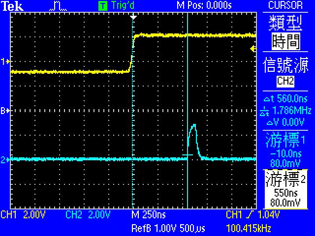
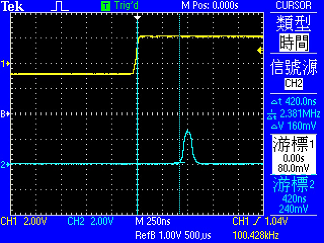
* Demo5: 量測 Interrupt Latency
* 使用 __attribute__( (naked) ) 去除 function stacking
- 有function stacking的延遲是560ns, 沒有的則是420ns,
- 因此function stacking: 560ns - 420ns = 140ns
```c
push {r7, lr}
add r7, sp, #0
pop {r7, pc}
```
/* Start running the tasks. */
vTaskStartScheduler();
- 再扣掉Toggle的反應時間
- Latency: 420ns - 80ns = 340ns
- 根據ARM Cortex-M4的文件,ISR stacking需12個cycle => 250ns
- pre-stacking delay = 340-250 = 90ns
return 0;
}
-------
- LED control task
.. code-block:: c
* interrupt latency = pre-stacking latency + 250ns + function stacking latency + toggle latency
- 560ns
static void LED_task(void *pvParameters)
{
RCC_ClocksTypeDef RCC_Clocks;
uint8_t togglecounter = 0x00;
-------
while(1)
{
/* Toggle LED5 */
STM_EVAL_LEDToggle(LED5);
vTaskDelay(100);
/* Toggle LED6 */
STM_EVAL_LEDToggle(LED6);
vTaskDelay(100);
}
}
- Button check task :
* interrupt latency without function stacking = pre-stacking latency + 250ns + toggle latency
- 420ns
.. code-block:: c
-------
static void button_task(void *pvParameters)
{
while (1)
{
/* Waiting User Button is pressed */
if (UserButtonPressed == 0x01)
{
/* Toggle LED4 */
STM_EVAL_LEDToggle(LED4);
vTaskDelay(100);
/* Toggle LED3 */
STM_EVAL_LEDToggle(LED3);
vTaskDelay(100);
}
/* Waiting User Button is Released */
while (STM_EVAL_PBGetState(BUTTON_USER) == Bit_SET);
UserButtonPressed = 0x00;
}
}
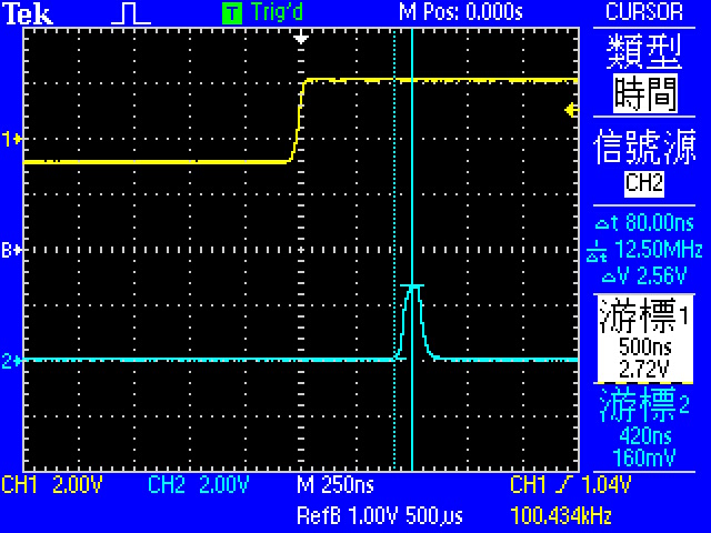
* Toggle latency = 80ns
- 0->1 的時間
Supplement
==========
- 一些有預設控制元件的腳位(詳見- STM32F4-Discovery 中文使用手冊P.16)
- LD3:橙色,連接到STM32F407VGT6的PD13
- LD4:綠色,連接到STM32F407VGT6的PD12
- LD5:红色,連接到STM32F407VGT6的PD14
- LD6:藍色,連接到STM32F407VGT6的PD15
- B1(USER):連接到STM32F407VGT6的PA0
- B2(RESET):連接到NRST,用於重置STM32F407VGT6
- 一些有預設控制元件的腳位
- LD3:綠色,連接到PG13
- LD4:紅色,連接到PG14
- B1(USER):連接到PA0
- B2(RESET):連接到NRST,用於重置
Q & A
=========
**1. Busy loop延遲的時間計算**
```c
int i=1000000;
while(i--);
```
編譯結果:(略去只執行一次的mov)
```c
80002d4: 687b ldr r3, [r7, #4]
80002d6: 1e5a subs r2, r3, #1
80002d8: 607a str r2, [r7, #4]
80002da: 2b00 cmp r3, #0
80002dc: d1fa bne.n 80002d4 <demo+0x34>
ldr : 2
subs : 1
str : 2
cmp : 1
ble.n: 1 or 1+P(pipeline refill)
```
若沒有branch,總共是2+1+2+1+1 = 7 cycle,
若有branch則是 2+1+2+1+2 = 8 cycle,(pipeline refill需要1~3 cycle,因alignment和instruction width而不同)
執行1000000次,也就是約8M個cycle,
經過實測時間為0.16秒,換算指令的執行頻率 = HCLK速度: 48Mhz (clock的速率請看下一節)
指令執行時間:Cortex-M4 instructions
[http://infocenter.arm.com/help/index.jsp?topic=/com.arm.doc.ddi0439b/CHDDIGAC.html](http://infocenter.arm.com/help/index.jsp?topic=/com.arm.doc.ddi0439b/CHDDIGAC.html)
* 關於STR, LDR系列指令,有cache機制可以在鄰近存取時減少執行時間
* Neighboring load and store single instructions can pipeline their address and data phases. This enables these instructions to complete in a single execution cycle.
--------
* System Clock與PLL

Reference Manual p.222 PLL_CFGR (DM00031020.pdf)
**CPU可以選擇HSE、HSI、PLL作為clock source,其中PLL是倍頻電路,可以HSE、HSI作為參考頻率做倍頻,配合除頻可以產生多種頻率組合。**
PLL會在Stop Standby Modes時被停用,HSE(or PLL)失效時會將System Clock改成HSI,並產生NMI exception,
主PLL -> HCLK -> Core,AHB,DMA,Memory (p.150還有其他的PLL供其他裝置使用)
專案預設設定:8Mhz / 25 * 300 / 2=48Mhz (`system_stm32f4xx.c`)
+ PLL_M [預設25] [可調範圍2~63]
+ PLL_N [預設300] [可調範圍192~432]
+ PLL_P [預設2] [可調範圍2 4 6 8]
+ PLL_Q [預設7] <-- to USB
Fref = HSE(8 Mhz) / PLL_M
VCO = Fref * PLL_N
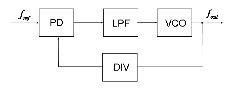
-----------
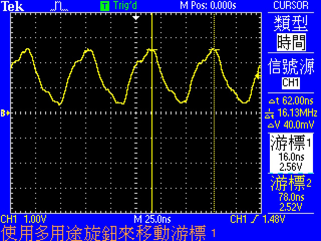
**alternate function中的MCO1(PA8), MCO2(PC9)可以將clock輸出到腳位上,用示波器測量得到以下結果**
---------------
- 8.065MHz, HSE
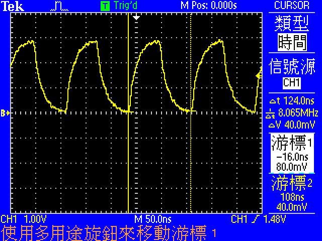
----------------
- 16.13MHz, HSI
Reference
=========
- `General Purpose Input/Output - Wikipedia, the free encyclopedia <http://en.wikipedia.org/wiki/General_Purpose_Input/Output>`_
- `STM32F407xx Datasheet<http://www.st.com/web/en/resource/technical/document/datasheet/DM00037051.pdf>`_
- `STM32F407xx Reference Manual<https://www.google.com.tw/url?sa=t&rct=j&q&esrc=s&source=web&cd=1&ved=0CCwQFjAA&url=http%3A%2F%2Fmeasure.feld.cvut.cz%2Fsystem%2Ffiles%2Ffiles%2Fcs%2Fvyuka%2Fpredmety%2FA4M38KRP%2FDM00031020.pdf&ei=Yd4tUrCbFIyZlQWy5IDAAw&usg=AFQjCNG98i1xkmhMAT5oY4owZfumzgq-3Q&sig2=BW3iz-5aJmyGhiu6HR32tA>`_
- `STM32F4-Discovery 中文使用手冊</embedded/STM32-Discovery-Manual-Chinese.pdf>`_
- `稀里糊塗學 STM32 第二講:源源不絕</embedded/learn-stm32-part-2.pdf>`_
- `GPIO PPT</embedded/GPIO_v3.ppt>`_
- [General Purpose Input/Output - Wikipedia, the free encyclopedia ](http://en.wikipedia.org/wiki/General_Purpose_Input/Output)
- [STM32F429xx Datasheet](http://www.st.com/web/en/resource/technical/document/datasheet/DM00071990.pdf)
- [STM32F42xxx Reference Manual](http://www.st.com/web/en/resource/technical/document/reference_manual/DM00031020.pdf)
- [STM32F429xx I/O pin mapping](http://mikrocontroller.bplaced.net/wordpress/wp-content/uploads/2013/10/Pinbelegung_f429_v100.html)
- [STM32F4-Discovery 中文使用手冊](/embedded/STM32-Discovery-Manual-Chinese.pdf)
- [稀里糊塗學 STM32 第二講:源源不絕](/embedded/learn-stm32-part-2.pdf)
- [給資工系的嵌入式電子學](https://embedded-note.hackpad.com/0KF0hrjt78j)
- [舊GPIO PPT](/embedded/GPIO_v3.ppt)
