General Purpose Input/Output (GPIO)
- Introduction - 簡介
- STM32F4xx GPIO特性
- Functional Description - 功能敘述
- Configuration - 配置圖
- Input configuration (P.273, 8.3.9 Input configuration in Reference manual)
- Output configuration (P.274, 8.3.10 Output configuration in Reference manual)
- Alternate function configuration (P.275, 8.3.11 Alternate function configuration in Reference manual)
- Analog configuration (P.276, 8.3.12 Analog configuration in Reference manual)
- Registers
- 暫存器
- Overview
- P.278, GPIO port mode register (GPIOx_MODER) in Reference manual
- P.279, GPIO port output type register(GPIOx_OTYPER) in Reference manual
- P.279, GPIO port output speed register (GPIOx_OSPEEDR) in Reference manual
- P.280, GPIO port pull-up/pull-down register (GPIOx_PUPDR) in Reference manual
- P.280, GPIO port input data register (GPIOx_IDR) in Reference manual
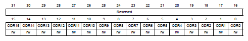
- P.281, GPIO port output data register (GPIOx_ODR) in Reference manual
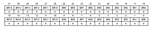
- P.281, GPIO port bit set/reset register (GPIOx_BSRR) in Reference manual
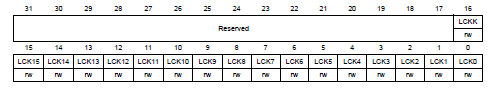
- P.281, GPIO port configuration lock register (GPIOx_LCKR) in Reference manual
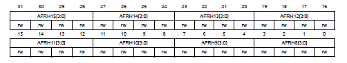
- P.283, GPIO alternate function low/high register(GPIOx_AFRL/GPIOx_AFRH) in Reference manual
- Demo - 測試實驗
- Supplement
- Q & A
- Reference
Introduction - 簡介
General Purpose Input/Output (GPIO)
a generic pin on an integrated circuit whose behavior, including whether
it is an input or output pin, can be controlled by the user at run
time.
- GPIO 是種具有彈性且可以藉由軟體控制 (software-controlled) 的數位訊號
- 常見於開發版邊緣, 以針腳 (Pin) 的形式呈現
- 這些針腳即是開發版與外界溝通的重要橋樑
- 簡單例子, 想像成是開關, 使用者可以打開或關閉 (input), 或由開發版來打開或關閉 (output)
- 每個 GPIO 可以被當成 input, output, analog 或 alternate function
- alternate function 是指其他的的功能, 如 I2C, SPI, USART, CCP, PWM, Clock 等。如何控制則取決於外部設備 (peripheral)
STM32F4xx GPIO特性
- 所有 GPIO 具有容許較高的電流能力與四種速度選擇,根據不同設定管理雜訊、電耗與電磁波
- 最大 I/O 切換速度可以支援到 90 MHz
- STM32F4xx 每個 GPIO Port 有 10 個 32-bit 暫存器 (Register)
- Configuration Register: GPIOx_MODER, GPIOx_OTYPER, GPIOx_OSPEEDR 與 GPIOx_PUPDR
- Data Register: GPIOx_IDR and GPIOx_ODR
- Set/Reset Register: GPIOx_BSRR
- Locking Register: GPIOx_LCKR 【防止因錯誤而改變GPIO的用途(accidental repurposing)】
- Alternate Function Selection Register: GPIOx_AFRH 與 GPIOx_AFRL
一個pin通常可被設定成input、output、alternate function或analog, (alternate function和analog只有在特定腳位)
input會有兩種狀態(floating, pull-up/down),output也有兩種狀態(push-pull, open drain with pull-up/down resistors)。
input/output方向 : input是指記憶體方接收來自設備的訊號源,output是指記憶體傳送訊號給設備。
各模式下的操作方式:
- Input mode:我們可以利用GPIO的input data register(GPIOx_IDR) 或是memory中提供給目標設備的data register (當設成alternate function的時候)去接收data。
- Output mode(非analog):GPIO提供output data register (GPIOx_ODR)及Bit set/reset register (GPIOx_BSRR)來對目標設備做控制
- Alternate function:此時要用memory中另外規劃給目標設備用的register對Pin腳進行控制。
- Analog mode:input和output會轉由adc/dac那邊做處理。
Functional Description - 功能敘述
input
- floating vs. pull-up/pull-down
當input pin被處在高阻抗的模式下,若沒有外部訊號源進來的話,此時是無法確定pin的狀態(不能確定現在處在高電位或低電位),除非有外部訊號來驅動電路。換句話說,input floating,這個input電位狀態完全是由外部訊號來決定,沒有訊號驅動的話,就會呈現高阻抗狀態。
剛剛提到floating在沒有外部訊號驅動的情況下是呈現高阻抗狀態(無法確定電位狀態=>不能明確表示現在值是0或1),如果我們需要這個pin有一個明確的預設狀態時,必須借助pull-up(pull-down)resistor來做調整,在pull-up resistor(pull-up外接高電壓,pull-down通常會接地)加入之下,讓pin的維持在明確的高電壓狀態(pull-down則是讓pin維持在低電壓狀態)。舉例來說,如果我們定電壓在3-4 V之間是1的狀態,0-1之間是0的狀態,高阻抗的時候,電壓是不明確的,有可能電壓值會落在1-3之間的不明確地帶,甚至是沒有在任何一個狀態維持一段時間,此時的狀態是未定的,但如果我們加入pull-up resistor的話,這個pin接受來自pull-up另一端的電壓供應,讓pin至少維持在3v以上時,我們就可以確定在沒有外部訊號驅動時,pin是維持在高電位狀態。
pull-up/pull-down電阻在大部分腳位上為40kΩ,在PA10/PB12上為10kΩ。至於其範圍,可以參考Datasheet p.110,Table 47. I/O static characteristics。
- 施密特觸發器(Schmitt trigger)
將類比訊號的波形整成數位電路所能處理的方波波形,以利被input register讀取(處理完只能分辨出高低電位的差別)。
 (施密特觸發器具有整流效果)
output
- push-pull vs open-drain mode
output處在push-pull模式下時,當output registers為”0”時輸出低電位,“1”時輸出高電位。而在open-drain模式下,“0”輸出低電位,“1”時為高阻抗(Z)狀態,電位無法確定。此兩種模式下,pin皆可pull-up/pull-down。
當有多個輸出pin在互相連通時(例如一個bus),若有兩個輸出呈不同狀態,電路上的電位便無法確定。因此,除了正在輸出的pin以外,其他pin應在高阻抗態以免干擾。以bus的例子來說,若令所有pin皆在open-drain mode pull-up,並使非輸出端pin為”1”(Z),當輸出pin為”1”時,bus為高電位(因為pull-up);當輸出pin為”0”時,bus為低電位。
analog
前面所述的input/output跟現在要談的類比模式是不一樣的類型,前者的資料型態主要是高低電位的數位型態(0/1的分別),而類比訊號是普遍自然界的訊號型態,故當我們設定成類比輸入的模式時,進來GPIO pin的原始訊號源在還沒經過施密特觸發器(Schmitt trigger)會有另一個線路將訊號做導向(通常是要導到ADC去),另一方面,當我們用了類比輸出模式後,GPIO的內部將會有一條線路接收DAC處理完的類比訊號,在經過此pin傳遞到外部去。
basic structure (P.266, Figure 25. Basic structure of a five-volt tolerant I/O port bit in Reference manual)
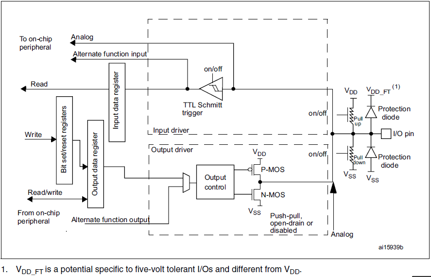 - VDD:晶片內部的工作電壓
- VDD_FT : I/O port專用電壓,與VDD不同 - VSS:接地點 - protection diode
: 防止輸入電壓超過一定範圍。當電壓低於VSS時,電流通過protection
diode流入pin;當電壓高於VDD_FT時,電流流出pin。
- VDD:晶片內部的工作電壓
- VDD_FT : I/O port專用電壓,與VDD不同 - VSS:接地點 - protection diode
: 防止輸入電壓超過一定範圍。當電壓低於VSS時,電流通過protection
diode流入pin;當電壓高於VDD_FT時,電流流出pin。
補充: TTL vs CMOS
- TTL由電阻器和三極體而組成,CMOS內部零件多以金屬氧化物半導體組成。
- 就早期而言,TTL的速度較CMOS快,但功耗較高。但近年來CMOS在速度方面已經超越TTL。
- TTL懸空一般會呈高電位,CMOS則為不定態。
Configuration - 配置圖
Input configuration (P.273, 8.3.9 Input configuration in Reference manual)
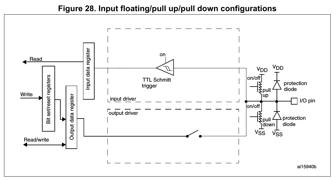 When
the I/O port is programmed as Input:
When
the I/O port is programmed as Input:
- the output buffer is disabled
- the Schmitt trigger input is activated
- 這種模式處理的數位訊號只在意高低電位的差別(開關控制)。
- the pull-up and pull-down resistors are activated depending on the
value in the GPIOx_PUPDR register
- 想要讓pin的state變成一個確定的狀態,可以設定pull-up/pull-down的使用。
- The data present on the I/O pin are sampled into the input data
register every AHB1 clock cycle
- input data的更新主要就是以AHB1本身的更新週期做決定,每一個cycle抵達時,data register就會根據當時Schmitt trigger整流完的狀態做更新。
- A read access to the input data register provides the I/O State
- 對data register的理解,我覺得用’狀態’比’數值’的敘述來的更好(大部分都是開關,就是外部訊號源是否有狀態改變,如 : button的按下與放開),而此處寫I/O state的意思是,即使我們現在是設成output(如 : LED控制),但我們仍然可用input data register來檢查LED現在的狀態。
Output configuration (P.274, 8.3.10 Output configuration in Reference manual)
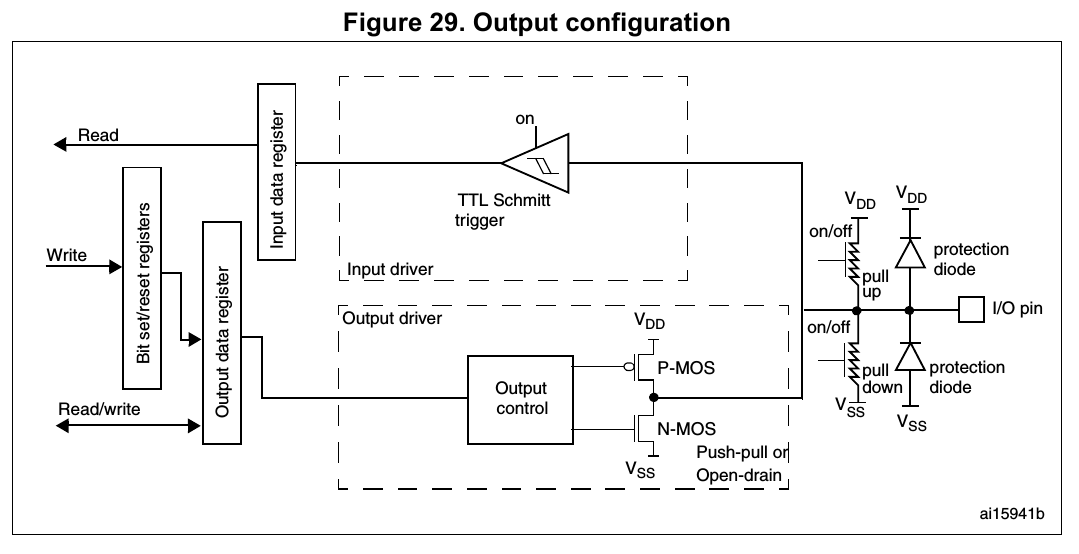 When
the I/O port is programmed as output:
When
the I/O port is programmed as output:
.. TODO: Output Control
- The output buffer is enabled:
- Open drain mode: A “0” in the Output register activates the N-MOS whereas a “1” in the Output register leaves the port in Hi-Z (the P-MOS is never activated)
- Push-pull mode: A “0” in the Output register activates the N-MOS whereas a “1” in the Output register activates the P-MOS
- 如前所述,設定Open drain / Push-pull的使用。
- The Schmitt trigger input is activated
- The weak pull-up and pull-down resistors are activated or not depending on the value in the GPIOx_PUPDR register
- The data present on the I/O pin are sampled into the input data register every AHB1 clock cycle
- A read access to the input data register gets the I/O state
- A read access to the output data register gets the last written
value
- 不一定與當下pin的狀態相同
Alternate function configuration (P.275, 8.3.11 Alternate function configuration in Reference manual)
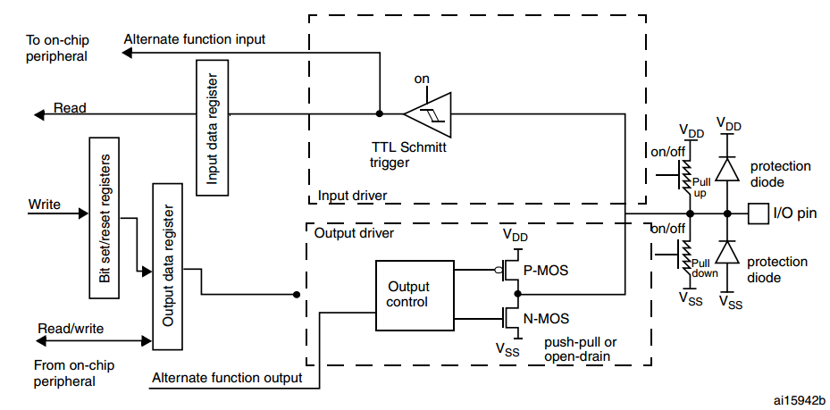 When the I/O
port is programmed as alternate function:
When the I/O
port is programmed as alternate function:
- The output buffer can be configured as open-drain or push-pull
- The output buffer is driven by the signal coming from the peripheral (transmitter enable and data)
- The Schmitt trigger input is activated
- The weak pull-up and pull-down resistors are activated or not depending on the value in the GPIOx_PUPDR register
- The data present on the I/O pin are sampled into the input data register every AHB1 clock cycle
- A read access to the input data register gets the I/O state
Remark:
GPIOx_AFRL[31:0] and GPIOx_AFRH[31:0] provide ways to select alternation functions. However, different alternate functions maps to different bits of ports. For more information, please refer to Table 12. Alternate function mapping from P.73 in STM32F429xx Datasheet.
Analog configuration (P.276, 8.3.12 Analog configuration in Reference manual)
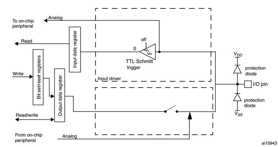 When the I/O port is
programmed as analog configuration:
When the I/O port is
programmed as analog configuration:
- The output buffer is disabled
- The Schmitt trigger input is deactivated, providing zero consumption for every analog value of the I/O pin. The output of the Schmitt trigger is forced to a constant value (0).
- The weak pull-up and pull-down resistors are disabled
- Read access to the input data register gets the value “0”
Note: In the analog configuration, the I/O pins cannot be 5 Volt tolerant. - analog operating voltage (VDDA) max at 3.6V
In analog to digital and digital to analog conversion of signals, the sampling is normally assumed to be periodic with a fixed period—the time between every two samples is the same. If there is jitter present on the clock signal to the analog-to-digital converter or a digital-to-analog converter, the time between samples varies and instantaneous signal error arises.
Registers - 暫存器
Overview
- Mode, Speed, Type, PuPd 對應表
P.278, GPIO port mode register (GPIOx_MODER) in Reference manual
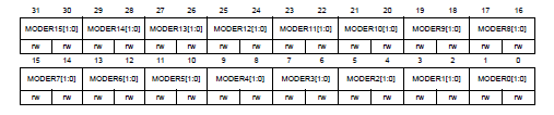 MODERy[1:0]決定第y pin
GPIO使用的configuration,2個bit為一組
MODERy[1:0]決定第y pin
GPIO使用的configuration,2個bit為一組
- 00: Input
- 01: output mode
- 10: Alternate function mode
- 11: Analog mode
- 當reset後,GPIOA_MODER=0xA800 0000、GPIOB_MODER=0x0000
0280,其他皆為0。
- PA3, PA4, PB13, PB14, PB15 為 Debug Pin in AF
P.279, GPIO port output type register(GPIOx_OTYPER) in Reference manual
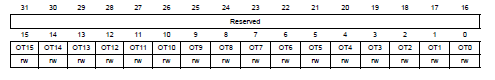 決定在output時使用的模式(如前面Functional Description.output所述)。
- 0: Output push-pull
- 1: Output open-drain
- reset皆為0x0000 0000
P.279, GPIO port output speed register (GPIOx_OSPEEDR) in Reference manual
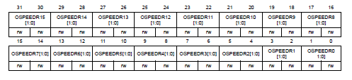 OSPEEDRy[1:0]決定output的速度。在不同的電容與電壓(VDD)下,輸出頻率可能不同,以下只列出代表值。
00: Low speed (2MHz)
01: Medium speed (10MHz)
10: Fast speed (50MHz)
11: High speed (100MHz)
reset GPIOB_OSPEEDR=0x0000 00C0,其他皆為皆為0x0000 0000
速度越高,雜訊與耗電量越多。
在其他狀態下的速度,可以參考 datasheet p134 table 58. I/O AC Characteristics
雜訊的來源
- Thermal noise 在電阻性的材料中,由於熱擾動的影響,造成材料內電子或電 洞等電荷載體產生隨機的速度擾動,這種類似布朗運動
- Shot noise 散粒雜訊通常存在于真空管中或半導體內,這種電子由負極到正極經外部電路的隨機運動 當電壓超過一定的臨界值而電流流出呈現散亂的形狀
P.280, GPIO port pull-up/pull-down register (GPIOx_PUPDR) in Reference manual
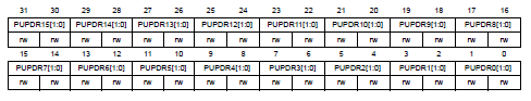 PUPDRy[1:0]決定pin
y是否pull-up/pull-down
PUPDRy[1:0]決定pin
y是否pull-up/pull-down
- 00: No pull-up, pull-down
- 01: Pull-up
- 10: Pull-down
- 11: Reserved
- reset GPIOA_PUPDR=0x6400 0000、GPIOB_PUPDR=0x0000 0100,其他0x0000 0000。
P.280, GPIO port input data register (GPIOx_IDR) in Reference manual
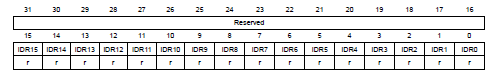 讀取IDRy為input
y的值。
讀取IDRy為input
y的值。
- Bits 31:16 Reserved, must be kept at reset value.
- Bits 15:0 IDRy: Port y input data
- register為read-only & word mode access only
- Reset: 0x0000 XXXX (X=undefined)
P.281, GPIO port output data register (GPIOx_ODR) in Reference manual
 輸出pin output的值。
- Bits 31:16 Reserved, must be kept at reset value.
- Bits 15:0 ODRy: Port output data
- Reset: 0x0000 0000
P.281, GPIO port bit set/reset register (GPIOx_BSRR) in Reference manual
 set或reset對應pin
output data register的值。
set或reset對應pin
output data register的值。
- Bits 31:16 BRy: reset bit y
- Bits 15:0 BSy: set bit y
- 0: no action ,1:set/reset
- write-only ,讀取會得到0
- Reset: 0x0000 0000
P.281, GPIO port configuration lock register (GPIOx_LCKR) in Reference manual
 若給bit
16(LCKK)一個正確的write sequence,可以鎖住bits
[15:0]對應的configurations。 當lock
sequence正確執行之後,GPIOx_LCKR在下次reset之前無法修改。
若給bit
16(LCKK)一個正確的write sequence,可以鎖住bits
[15:0]對應的configurations。 當lock
sequence正確執行之後,GPIOx_LCKR在下次reset之前無法修改。
- Bit 16 LCKK[16]: Lock key
- 0: Port configuration lock key not active
- 1: Port configuration lock key active
- 只能在lock sequence時寫入
- Bits 15:0 LCKy: lock bit y
- 0: Port configuration not locked
- 1: Port configuration locked
- Lock sequences pseudocode
WR LCKR[16] = ‘1’ + LCKR[15:0]
WR LCKR[16] = ‘0’ + LCKR[15:0]
WR LCKR[16] = ‘1’ + LCKR[15:0]
RD LCKR
RD LCKR[16] = ‘1’ (optional, confirm only)- Lock sequences in c lib (
STM32F4xx_StdPeriph_Driver/src/stm32f4xx_gpio.c:void GPIO_PinLockConfig())
tmp |= GPIO_Pin;
/* Set LCKK bit */
GPIOx->LCKR = tmp;
/* Reset LCKK bit */
GPIOx->LCKR =  GPIO_Pin;
/* Set LCKK bit */
GPIOx->LCKR = tmp;
/* Read LCKK bit*/
tmp = GPIOx->LCKR;
/* Read LCKK bit*/
tmp = GPIOx->LCKR;
在執行中,LCK[15:0]的值不可改變,否則lock失敗。
P.283, GPIO alternate function low/high register(GPIOx_AFRL/GPIOx_AFRH) in Reference manual
 選擇pin y的alternate
function。
選擇pin y的alternate
function。
- AFRLy/AFRHy : Alternate function selection for bit y
- AFRLy/AFRHy = 0000~1111 分別對應AF0~AF15
參考 Datasheet p.73~83 對照表,一個Pin可以對應一個alternate function
Demo - 測試實驗
實驗設備
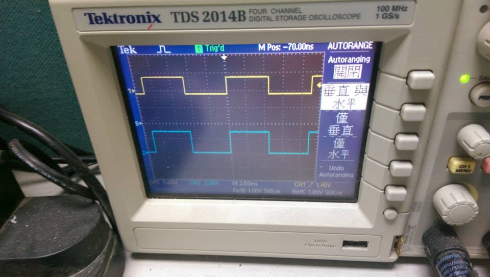
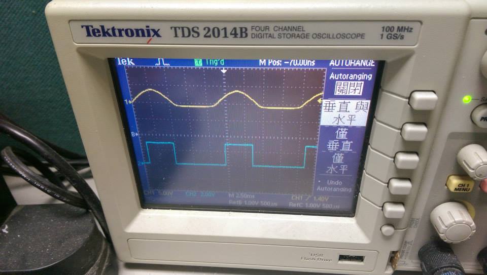
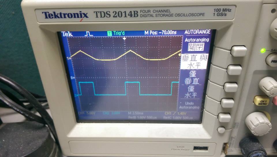
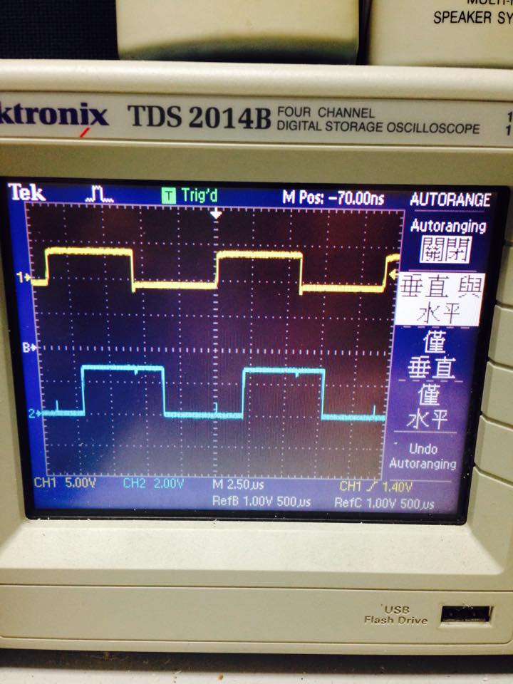
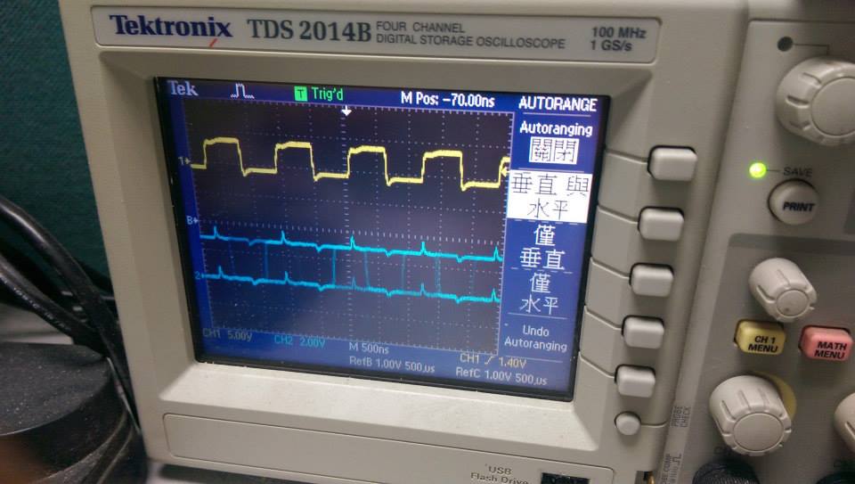
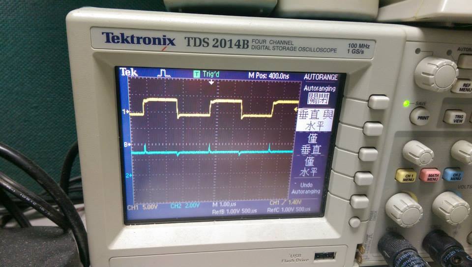
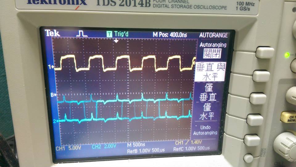
- 除了STM32本身外,我們使用一台訊號產生器與一台示波器。
- 將訊號產生器輸出(+)接到示波器的channel 1(黃色)與
PG9,STM32的輸出PG13接示波器的channel 2(藍色)
- demo3, demo4
- 訊號產生器的接地(-)接到STM32的GND與示波器channel 1/2的負極。
- 90.9Hz ,方波
- 起始狀態,程式將 PG9 的輸入 GPIOA_IDR shift 後送到 GPIOG_ODR,由
PG13 輸出。
- demo3, demo4
- 90.9Hz ,sin波
- 90.9Hz ,三角波
- 87000HZ ,interrupt with function call
- visible interrupt delay ,about 2000ns
- demo4 使用 GPIO_ToggleBits 切換
- 833000Hz ,interrupt with function call
- 頻率再增加, 會造成無法正常的解析波形
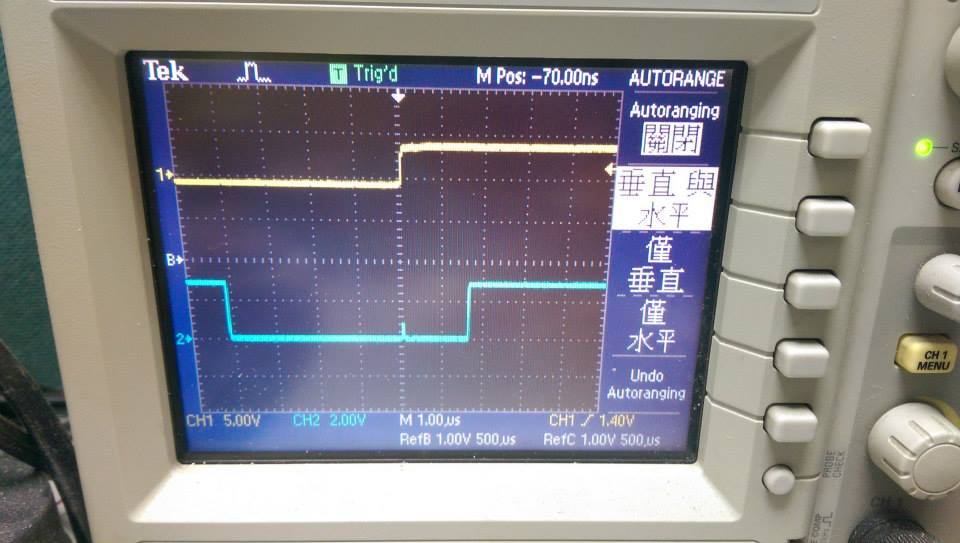
- polling with function call
- 使用polling的結果,delay大約750ns
- demo3 使用 GPIO_ToggleBits 切換
- 與 demo4 相比會波型會抖動
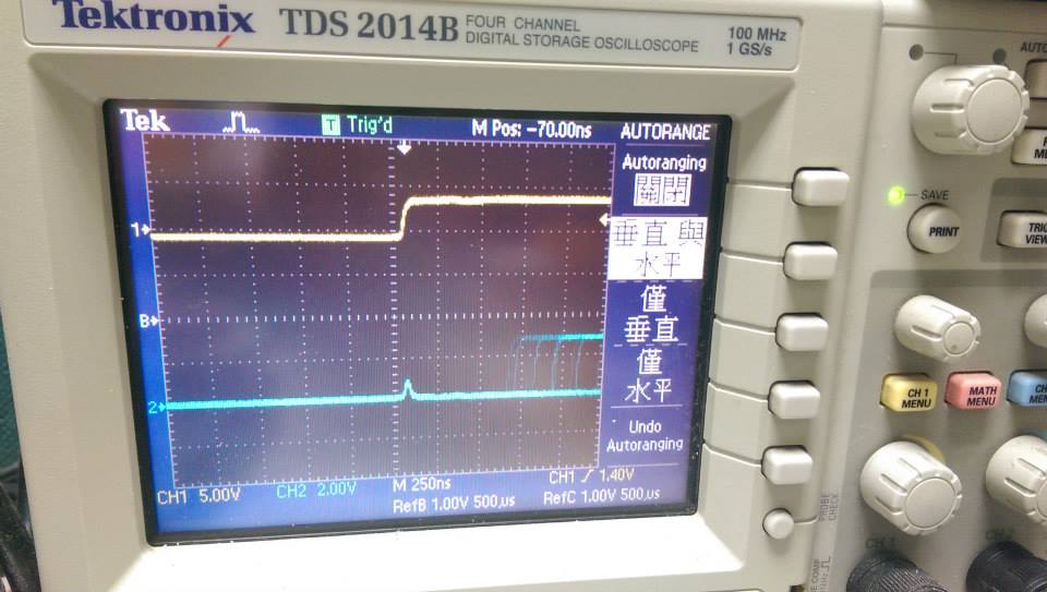
- 88500Hz ,interrupt without function call
- interrupt不用function call,delay大約1500ns
- demo4 使用 GPIOG->ODR = GPIOA->IDR << 13; 切換
- polling without function call
- 不用function call,delay大約250ns
- demo3 使用 GPIOG->ODR = GPIOA->IDR << 13; 切換
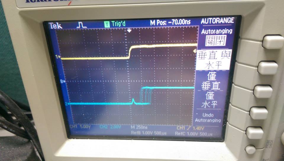
- 260000Hz ,interrupt without function call
- 頻率加快的結果
- demo4
- 波型呈現連續都是高電位
- 1111000Hz ,interrupt without function call
- 頻率再增加的結果
- demo4
- 波型開始呈現交錯, 主要是因為偵測時會有交錯
- 一般的下拉電阻

- PA10 /PB12 的例外電阻
Code Section - 程式碼
sample code download :
Demo 範例選擇 :
- 共有
demo1.c,demo2.c,demo3.c,demo4.c - 請在
main.c修改需要執行的 demo 範例 (同時間只能選擇其中一個範例)
配置說明 :
- STM32F429I-Discovery Library 的預先定義(in
STM32F429I-Discovery/stm32f429i_discovery.h) :
#define LED4_PIN                         GPIO_Pin_13
#define LED4_GPIO_PORT                   GPIOG
#define LED4_GPIO_CLK                    RCC_AHB1Periph_GPIOG

#define LED3_PIN                         GPIO_Pin_14
#define LED3_GPIO_PORT                   GPIOG
#define LED3_GPIO_CLK                    RCC_AHB1Periph_GPIOG

#define USER_BUTTON_PIN                GPIO_Pin_0
#define USER_BUTTON_GPIO_PORT          GPIOA
#define USER_BUTTON_GPIO_CLK           RCC_AHB1Periph_GPIOA
#define USER_BUTTON_EXTI_LINE          EXTI_Line0
#define USER_BUTTON_EXTI_PORT_SOURCE   EXTI_PortSourceGPIOA
#define USER_BUTTON_EXTI_PIN_SOURCE    EXTI_PinSource0
#define USER_BUTTON_EXTI_IRQn EXTI0_IRQn - LED 配置
- Port: G
- Pin: 13、14。
- CLK: RCC_AHB1Periph_GPIOG
- Button 配置
- Port: A
- Pin: 0
- CLK: RCC_AHB1Periph_GPIOA
- 以上資訊也可以從架構圖, Pin Mapping 與開發版上的標示得知
初始化設定 :
- RCC 參數設置, 根據需要使用到的 GPIO Port 與 Bus 來初始化對應的 CLK
- 以下範例為初始化 GPIO Port: G; GPIO Bus: AHB1
- 此對應的 CLK 的相對名稱為 RCC_AHB1Periph_GPIOG
- 以下範例為初始化 GPIO Port: G; GPIO Bus: AHB1
- GPIO 參數設置, 設定 Pin, Mode, Type, Pull-Up/Pull-Down, Speed
- 根據不同的 Mode, 設置不同對應的參數, 並非所有的資料都需要設置
- 以下範例為初始化 LED3 與 LED4, GPIO Port: G; Pins: 13, 14; Mode: Output; Type: Push-Pull; Pull-Up/Pull-Down: No Pull; Speed: 2MHz
- 詳細參數名稱可參考
STM32F4xx_StdPeriph_Driver/inc/stm32f4xx_gpio.h
// GPIO Configuration
// LED3 (Green): GPIO_Pin_13, LED4 (Red): GPIO_Pin_14
GPIO_InitTypeDef GPIO_InitStructure;
GPIO_InitStructure.GPIO_Pin = GPIO_Pin_13 | GPIO_Pin_14;
GPIO_InitStructure.GPIO_Mode = GPIO_Mode_OUT;
GPIO_InitStructure.GPIO_OType = GPIO_OType_PP;
GPIO_InitStructure.GPIO_PuPd = GPIO_PuPd_NOPULL;
GPIO_InitStructure.GPIO_Speed = GPIO_Speed_2MHz;
GPIO_Init(GPIOG, &GPIO_InitStructure);- Interrupt 參數設置
- 所有的 Port 都可以有 external interrupt
- 使用 external interrupt 必須設置為 input
- 以下範例設置 GPIO Port: A; Pin: 0
- 根據設置我們可以得知此 GPIO 對應的是 User Button
- 詳細參數名稱可參考
STM32F4xx_StdPeriph_Driver/inc/stm32f4xx_syscfg.h
- 所有的 Port 都可以有 external interrupt
EXTI_InitTypeDef EXTI_InitStructure;
NVIC_InitTypeDef NVIC_InitStructure;

/* Connect EXTI Line 0 to the button GPIO Pin */
SYSCFG_EXTILineConfig(EXTI_PortSourceGPIOA, GPIO_PinSource0);

/* Configure the EXTI line to generate an interrupt when the button is
 * pressed. The button pin is high when pressed, so it needs to trigger
 * when rising from low to high. */
EXTI_InitStructure.EXTI_Line = EXTI_Line0;
EXTI_InitStructure.EXTI_Mode = EXTI_Mode_Interrupt;
EXTI_InitStructure.EXTI_Trigger = EXTI_Trigger_Rising_Falling;
EXTI_InitStructure.EXTI_LineCmd = ENABLE;
EXTI_Init(&EXTI_InitStructure);

/* Enable and set Button EXTI Interrupt to the lowest priority */
NVIC_InitStructure.NVIC_IRQChannel = EXTI0_IRQn;
NVIC_InitStructure.NVIC_IRQChannelPreemptionPriority = 0x0F;
NVIC_InitStructure.NVIC_IRQChannelSubPriority = 0x0F;
NVIC_InitStructure.NVIC_IRQChannelCmd = ENABLE;
NVIC_Init(&NVIC_InitStructure);- Interrupt Handler 設置
- 根據上述設定, 對應的 Interrupt Handler 為 EXTI0_IRQHandler
- 可在對應的 Handler 實作
- 根據上述設定, 對應的 Interrupt Handler 為 EXTI0_IRQHandler
void EXTI0_IRQHandler(void)
{
    if(EXTI_GetFlagStatus(EXTI_Line0) != RESET)
    {
        // To do something in here

        /* Clear the EXTI line pending bit */
        EXTI_ClearITPendingBit(EXTI_Line0);
    }
}- Demo1
- 兩個 LED 燈交互閃爍
- 初始化 PG13 (GPIO Port: G; Pin: 13), PG14 為 Output
- 可以使用 GPIO_ToggleBits (in
STM32F4xx_StdPeriph_Driver/inc/stm32f4xx_gpio.c)- 此部份需要注意 delay 時間, 若設置太短則不易辨識
- 由於預設的 HCLK 速度則是 48Mhz
- for(int i=0; i<1000000; i++) 總共是 10 cycle
- 因此延遲時間約 0.27 秒
- 兩個 LED 燈交互閃爍
void demo1()
{
    RCC_Configuration_Demo1();
    GPIO_Configuration_Demo1();

    GPIO_ToggleBits(GPIOG, GPIO_Pin_14);

    while(1)
    {
        GPIO_ToggleBits(GPIOG, GPIO_Pin_13);
        GPIO_ToggleBits(GPIOG, GPIO_Pin_14);

        // Delay
        for(int i=0; i<1000000; i++);
    }
} - Demo2
- LED3 由 User Button 控制閃爍, LED4 持續閃爍
- 初始化 PG13 (GPIO Port: G; Pin: 13), PG14 為 Output
- 初始化 external interrupt 為 PA0
- LED3 由 User Button 控制閃爍, LED4 持續閃爍
void EXTI0_IRQHandler(void)
{
    if(EXTI_GetFlagStatus(EXTI_Line0) != RESET)
    {
        GPIO_ToggleBits(GPIOG, GPIO_Pin_13);
        EXTI_ClearITPendingBit(EXTI_Line0);
    }
}

void demo2()
{
    RCC_Configuration_Demo2();
    GPIO_Configuration_Demo2();
    Interrupts_Configuration_Demo2();

    while(1)
    {
        GPIO_ToggleBits(GPIOG, GPIO_Pin_14);

        // Delay
        for(int i=0; i<1000000; i++);
    }
}- Demo3
- LED3 利用 Polling 方式來探測外部訊號改變閃爍
- 閃爍部份則直接將 IDR 配置到 ODR
- 初始化 PG13 為 Output, PG9 為 Input
void demo3()
{
    RCC_Configuration_Demo3();
    GPIO_Configuration_Demo3();

    while(1)
    {
        // GPIO read IDR and assign to ODR
        GPIOG->ODR = GPIOA->IDR << 13;
    }
}- Demo4
- LED3 利用 external interrupt 方式來探測外部訊號改變閃爍
- 閃爍部份則直接將 IDR 配置到 ODR
- 初始化 PG13 為 Output, PG9 為 Input
void EXTI0_IRQHandler(void)
{
    if(EXTI_GetFlagStatus(EXTI_Line1) != RESET)
    {
        GPIOG->ODR = GPIOG->IDR << 13;
        EXTI_ClearITPendingBit(EXTI_Line1);
    }
}

void demo4()
{
    RCC_Configuration_Demo4();
    GPIO_Configuration_Demo4();
    Interrupts_Configuration_Demo4();

    while(1);
}- Demo5: 量測 Interrupt Latency
- 使用 attribute( (naked) ) 去除 function stacking
- 有function stacking的延遲是560ns, 沒有的則是420ns,
- 因此function stacking: 560ns - 420ns = 140ns
- 再扣掉Toggle的反應時間
- Latency: 420ns - 80ns = 340ns
- 根據ARM Cortex-M4的文件,ISR stacking需12個cycle => 250ns
- pre-stacking delay = 340-250 = 90ns
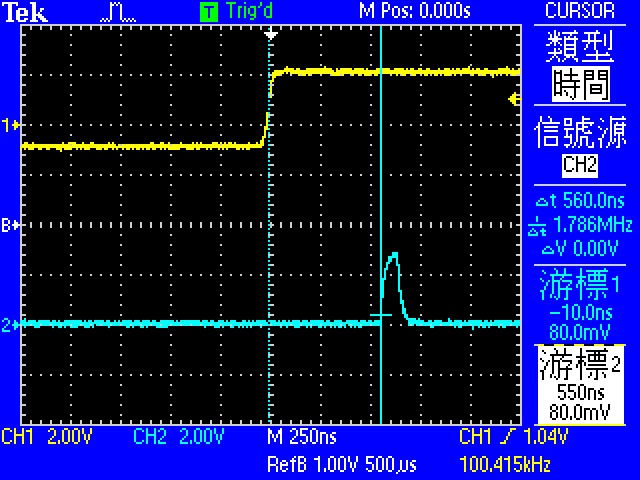
- interrupt latency = pre-stacking latency + 250ns + function stacking
latency + toggle latency
- 560ns
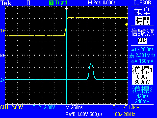
- interrupt latency without function stacking = pre-stacking latency +
250ns + toggle latency
- 420ns
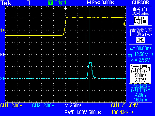
- Toggle latency = 80ns
- 0->1 的時間
Supplement
- 一些有預設控制元件的腳位
- LD3:綠色,連接到PG13
- LD4:紅色,連接到PG14
- B1(USER):連接到PA0
- B2(RESET):連接到NRST,用於重置
Q & A
1. Busy loop延遲的時間計算
編譯結果:(略去只執行一次的mov)
80002d4:       687b            ldr     r3, [r7, #4]
80002d6:       1e5a            subs    r2, r3, #1
80002d8:       607a            str     r2, [r7, #4]
80002da:       2b00            cmp     r3, #0
80002dc:       d1fa            bne.n   80002d4 <demo+0x34>

ldr  : 2
subs : 1
str  : 2
cmp  : 1
ble.n: 1 or 1+P(pipeline refill)
若沒有branch,總共是2+1+2+1+1 = 7 cycle, 若有branch則是 2+1+2+1+2 = 8 cycle,(pipeline refill需要1~3 cycle,因alignment和instruction width而不同) 執行1000000次,也就是約8M個cycle, 經過實測時間為0.16秒,換算指令的執行頻率 = HCLK速度: 48Mhz (clock的速率請看下一節)
指令執行時間:Cortex-M4 instructions http://infocenter.arm.com/help/index.jsp?topic=/com.arm.doc.ddi0439b/CHDDIGAC.html
- 關於STR, LDR系列指令,有cache機制可以在鄰近存取時減少執行時間
- Neighboring load and store single instructions can pipeline their address and data phases. This enables these instructions to complete in a single execution cycle.
- System Clock與PLL

Reference Manual p.222 PLL_CFGR (DM00031020.pdf)
CPU可以選擇HSE、HSI、PLL作為clock source,其中PLL是倍頻電路,可以HSE、HSI作為參考頻率做倍頻,配合除頻可以產生多種頻率組合。
PLL會在Stop Standby Modes時被停用,HSE(or PLL)失效時會將System Clock改成HSI,並產生NMI exception,
主PLL -> HCLK -> Core,AHB,DMA,Memory (p.150還有其他的PLL供其他裝置使用)
專案預設設定:8Mhz / 25 * 300 / 2=48Mhz
(system_stm32f4xx.c)
- PLL_M [預設25] [可調範圍2~63]
- PLL_N [預設300] [可調範圍192~432]
- PLL_P [預設2] [可調範圍2 4 6 8]
- PLL_Q [預設7] <– to USB
Fref = HSE(8 Mhz) / PLL_M
VCO = Fref * PLL_N
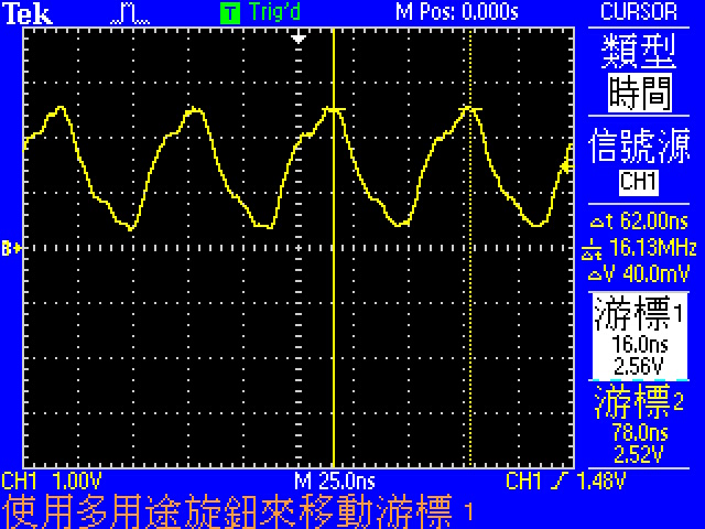
alternate function中的MCO1(PA8), MCO2(PC9)可以將clock輸出到腳位上,用示波器測量得到以下結果
- 8.065MHz, HSE
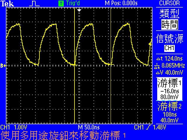
- 16.13MHz, HSI