FreeRTOS (MMU)
協作者
共筆
目錄
Beaglebone black 簡介
硬體簡介
- Processor: AM335x 1GHz
ARM® Cortex-A8
- 512MB DDR3 RAM
- 4GB 8-bit eMMC on-board flash storage
- 3D graphics accelerator
- NEON floating-point accelerator
- 2x PRU 32-bit microcontrollers
- Connectivity
- USB client for power & communications
- USB host
- Ethernet
- HDMI
- 2x 46 pin headers
- Software Compatibility
- Debian
- Android
- Ubuntu
- Cloud9 IDE on Node.js w/ BoneScript library
- plus much more

開機流程
當Beaglebone Black(BBB)一上電後,即開始執行ROM裡面的ROM code。再來根據腳位SYSBOOT的值來決定讀取哪裡的MLO檔,預設是讀取板子上eMMC的MLO檔。再來靠MLO讀取u-boot,u-boot再根據文件uEnv.txt載入image或file system。
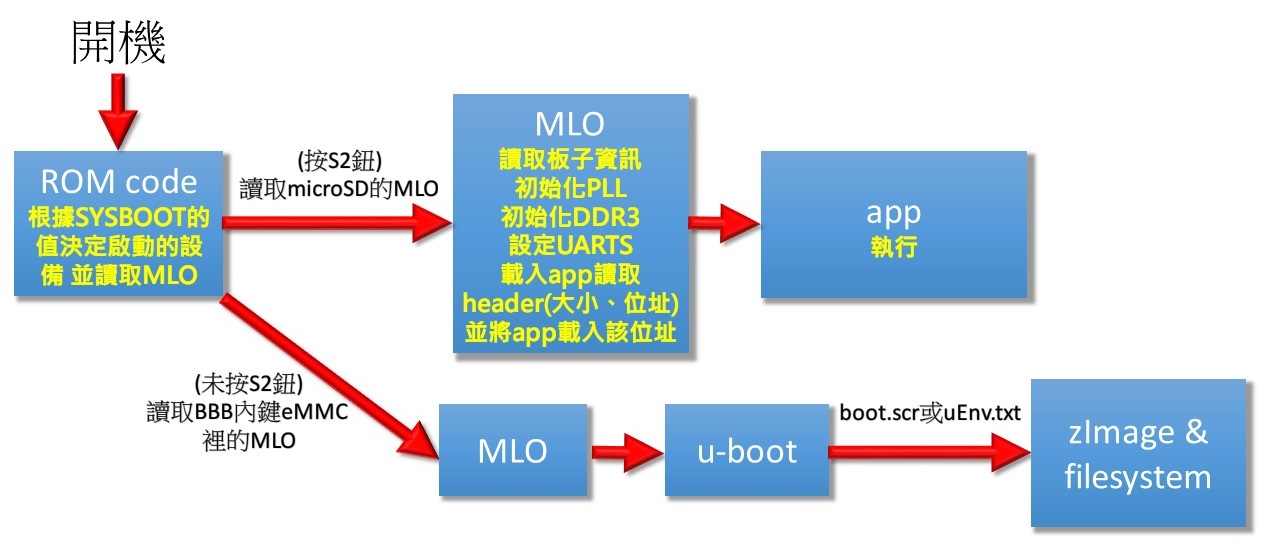
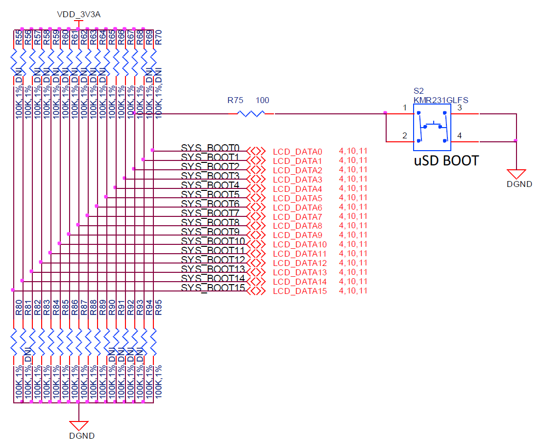
若是按住BBB板子上的S2按鍵,根據下圖,會讓SYS_BOOT2變成低電位,使得BBB的ROM code載入MMCSD內的MLO並執行。之後再根據MLO的程式碼來決定要載入什麼檔案執行。在我們第一次實驗時,是利用MLO去載入app並執行。
FreeRTOS on Beaglebone Black
開發環境
- 主機環境:Ubuntu 14.10、Linux Mint 17
- 開發板:Beaglebone black (Rev C)
- Cross compiler: https://launchpad.net/gcc-arm-embedded/+download 下載並解壓至喜歡的地方
實作過程
下載程式碼:
.. code-block:: bash
git clone https://github.com/henfos/BBBFreeRTOS.git
cd BBBFreeRTOS/Demo/AM3359_BeagleBone_GCC
修改 main.c ,在開頭補上 :
.. code-block:: c
#include <stdint.h>
設定環境變數 :
.. code-block:: bash
export PATH=(cross compiler 解壓縮路徑)/gcc-arm-none-eabi-xxxxxxxx/bin:$PATH
export LIB_PATH=(cross compiler 解壓縮路徑)/gcc-arm-none-eabi-xxxxxxxx
修改 makefile:
將以下原本的參數
.. code-block:: makefile
CC=/home/henrifo/Nedlastinger/gcc-arm-none-eabi-4_8-2013q4/bin/arm-none-eabi-gcc
OBJCOPY=/home/henrifo/Nedlastinger/gcc-arm-none-eabi-4_8-2013q4/bin/arm-none-eabi-objcopy
ARCH=/home/henrifo/Nedlastinger/gcc-arm-none-eabi-4_8-2013q4/bin/arm-none-eabi-ar
改成
.. code-block:: makefile
    CC=arm-none-eabi-gcc
    OBJCOPY=arm-none-eabi-objcopy
    ARCH=arm-none-eabi-ar
接下來執行make,會產生 rtosdemo-a.bin
編寫uEnv.txt讓u-boot根據其而載入rtosdemo-a.bin,內容如下
.. code-block:: txt
bootcmd=fatload mmc 0 0x80500000 rtosdemo-a.bin; go 0x80500000;
uenvcmd=boot
將MLO、uEnv.txt、u-boot.img、rtosdemo-a.bin放入MicroSD卡
按住BBB的S2鈕並開機
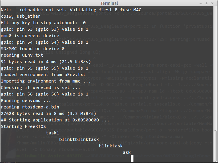
結果圖如下,可看出FreeRTOS已能初步運作。
將main.c的3個task,刪減到剩下1個。 將delay的計數器從0x1FFF改成0x3FF0000,增加閃爍時間間隔。 並將serial_puts的function中加入’\r’,將輸出的游標推到每行起始位置。
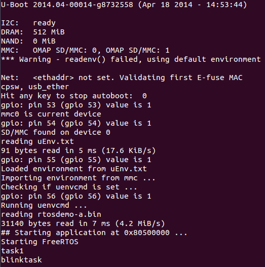
結果圖如下,輸出的結果比較清晰且LED的閃爍可以用肉眼察覺。
移植FreeRTOS 8.2.1到BBB
到FreeRTOS官網下載8.2.1版 (目前最新版本)的source
解壓後將8.2.1版本的source資料夾替換掉原本的source後,再來將原本的Source/portable/GCC/AM335_BeagleBone複製回去。
然後接著修改Source/include資料夾底下的portable.h檔
將
.. code-block:: header file
#ifdef GCC_AM335_BeagleBoard
    #include "../../Source/portable/GCC/AM335_BeagleBone/portmacro.h"
#endif
加至
.. code-block:: header file
#ifndef portENTER_CRITICAL
    #include "portmacro.h"
#endif
的前面,以免發生錯誤。
接著修改Source/portable/GCC/AM335_BeagleBone底下的portmacro.h
在裡面加入
.. code-block:: header file
typedef portSTACK_TYPE  StackType_t;
typedef long BaseType_t;
typedef unsigned long UBaseType_t;
typedef uint32_t TickType_t;
並將下面的 portTICK_RATE_MS 改為 portTICK_PERIOD_MS
修改Source/portable/GCC/AM335_BeagleBone/portISR.c檔案裡的vTaskIncrementTick改為xTaskIncrementTick (165行)
出現結果與上圖相同,但仍有許多warning需解決。
UART I/O
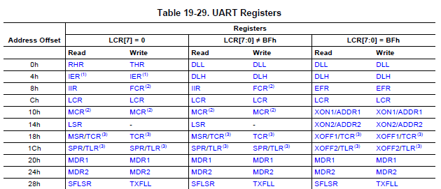
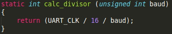
初始化設定:
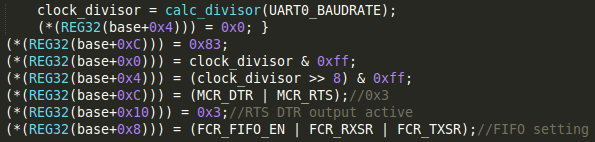
IER[4]設為0(sleep mode),才可設定DLL與DLH,接著將LCR[7]設為1,base+0x0和base+0x4的位置會對應到DLL、DLH,接著設定DLL與DLH(baud rate 相關設定),再將LCR[7]設為0 接著RTS DTR output active(傳輸的通知訊號)

ARMv7-A MMU Architecture
Sections and pages
ARM 的 MMU 支援 四種 page sizes(比較大的稱 section,比較小的稱 pages )
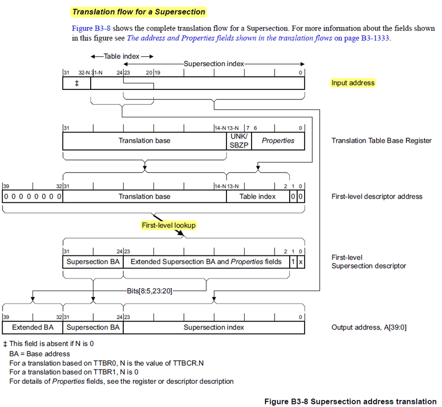
Supersections: 16 MB memory blocks (24-bit offsets)
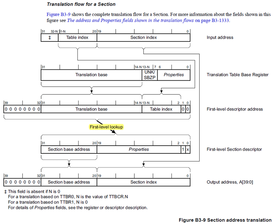
Sections: 1 MB memory blocks (20-bit offsets)
Large pages: 64 KB pages (16-bit offsets)
Small pages: 4 KB pages (12-bit offsets)
The MMU supports a two-level hierarchy for its page table structure.
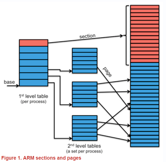
first-level table 功能:
- 包含pointer,指向 second-level tables
- 當做 section 或 supersection 的 base address
Translation Lookaside Buffers (TLB)
TLB分為以下兩種:
- Micro TLB (The first-level TLB)
- Main TLB (The second-level TLB)
Micro TLB 特色介紹:
- 最小也最快
- 分成兩部分,for instruction 和 for data
- can store 32 entries
- fully associative and can perform a lookup in one clock cycle
- 使用 address space identifier(ASID)
- Allow the operating system to identify one process’ address space from another’s without flushing the cache.
- 避免當Task Context-Switch發生時,TLB被Flush的成本
- Entries can also be tagged as global –> shared
- 每一個 entry 都有 protection bits, 用來確認每一個 address lookup
- 如果 protections 不允許記憶體存取,則 MMU會發出 Data Abort 的訊號,將會造成一個 trap
- 發生cache miss時,replacement algorithm 可能採用 round-robin (the default) 或 random replacement 的 policy
Main TLB 介紹:
- 使用時機: cache misses from the microTLBs
- 他只有一個,意味著 Main TLB 要處理 data-side 或是 instruction-side MicroTLBs 產生的 misses
- eight-way set associative with 64-byte blocks and 1 MB capacity
- 每個Main TLB項目都會包括
- Virtual Address
- Page Size
- Physical Address
- Memory Properties
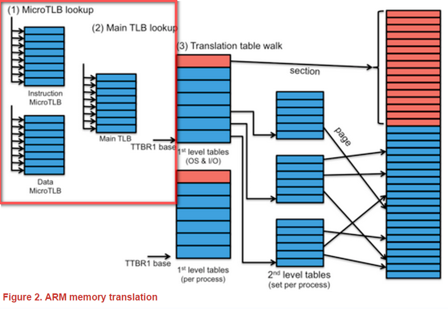
Figure 2 表示出所有 elements 運作流程:
第一步是在 MicroTLB . Instruction fetch 時存取 Instruction MicroTLB 以及在 data read/write operation時去存取Data MicroTLB。 一個資料被存取除了查表要查的到以外,還需要access permission,如果沒有 proper permissions,會產生 trap (Data Abort signal)。如果發生 miss,就會到step 2 ( 去 lookup Main TLB )。
當 MicroTLB lookup 產生 cache miss,會往 Main TLB去找. Lookup過程與 MicroTLB相同(matched requested page and permissions)。如果 miss,到 step 3.
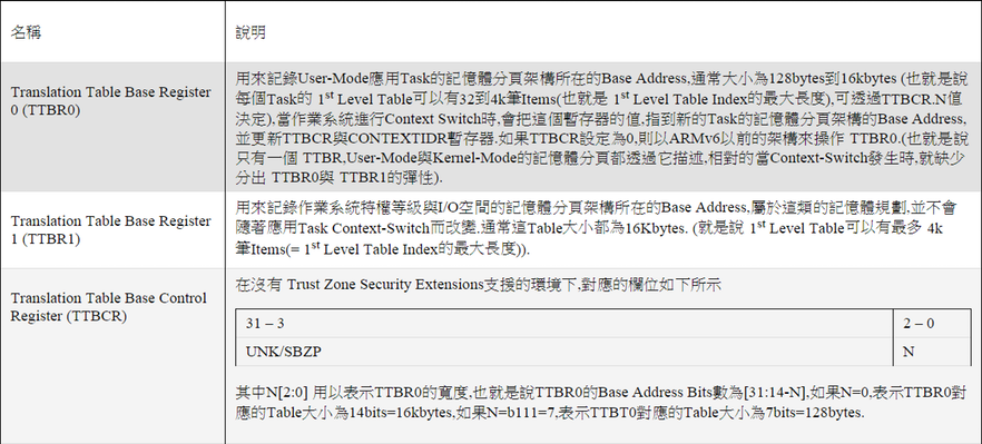
最後的 step 是 page table(s) (在此稱為 translation table work)。系統支援 2個 first-level tables。VA 的 high-order bits 決定使用哪一個 table。根據VA的 topmost n bits是0(用 TTBR0)或者不是0(用TTBR1)。而 n 的值取決於Translation Table Base Control Register (TTBCR)。operating system 和 memory-mapped I/O 位於 upper part of the address space 並被 TTBR1 管理。user processes 在 lower part of memory 並被 TTBR0 管理。當在context switch時,operating system 為了新的 process, 必須切換到TTBR0去指向first-level table 。TTBR0仍將保留operating system 和 memory-mapped I/O 的 memory map。
經由記憶體中page table來查找位址被稱為translation table walk,因為它可能涉及經過不同階層的table。藉由ARM MMU,section可由first-level page table直接對應出位址;page則是兩步驟的過程。如果是section,則實體基準位址是被儲存在first-level table的page table entry中,若是page,則是second-level table的位址儲存在first-level table的page table entry中。
以ARMv7架構為例,要控制TLB Translation Table,可以透過CP15的暫存器c2,其中c2主要提供以下Translation table base registers
下面來談談根據TLB的設定參數組合,分別以基於16MB(SuperSection),1MB(Section),64KB(Large Page),4KB(Small Page)不同分頁的組合,來說明TLB 1級與2級 Table的運作概念,
如下所示為16MB(SuperSection) 配置下,TLB分頁運作的概念
如下所示為1MB(Section) 配置下,TLB分頁運作的概念
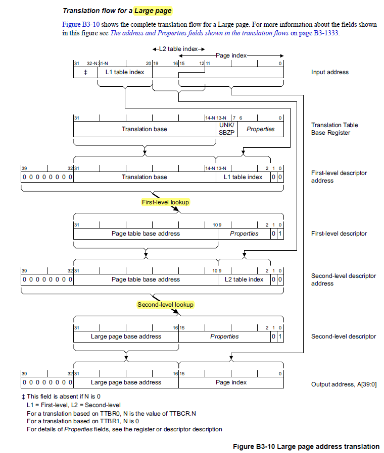
如下所示為64KB(Large Page) 配置下,TLB分頁運作的概念
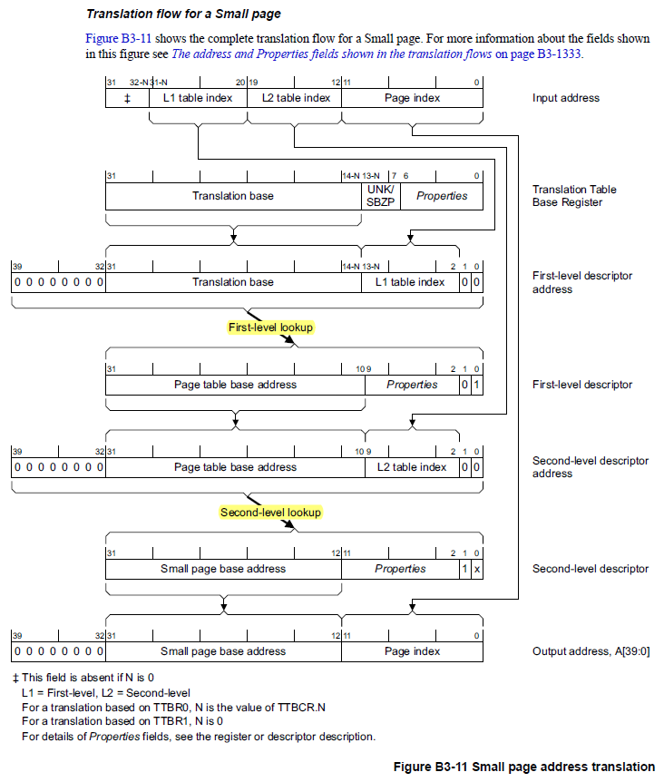
如下所示為4KB(Small Page) 配置下,TLB分頁運作的概念
保護機制與記憶體行為
每次記憶體存取都會跟每個記憶體區塊的page table entry中儲存的權限做確認,無論是page還是section都是。而且page table entry還可以指定一個記憶體區域中對於其他核心或處理器來說的記憶體被修改的可見性。記憶體區域可以有以下特性:
- Execute never: 阻止處理器中的指令去存取這個區域的記憶體
- Read-only, read/write, no access: 這幾個模式可在user-mode和privileged (kernel) mode中做不同設定。例如,kernel 的記憶體可被標示為user mode不能存取,但kernel mode可以讀寫。
- non-secure: 標示記憶體區域為”信任的”
- sharable: 這個可以標示是否一個區域的記憶體可以與其他處理器共用,或是可以映射到硬體裝置。有以下幾種模式可以被設定:
- Strongly ordered: 記憶體存取必須根據程式執行的順序
- Device/shared or device/non-shared: 這記憶體是直接對應到硬體裝置(因此沒有快取),且這個裝置是否與其他處理器在匯流排中共享。
- normal/shared, normal/non-shared: 一般的記憶體使用,再來看可否在與其他處理器在匯流排上共享。
若是記憶體存取沒有通過權限,MMU會發出Memory Abort訊號給處理器。
ARMv7-A 啟用MMU設定
MMU 可以透過 system control coprocessor (CP15) registers 進行設定 (reference here)
CP15 又稱系統控制協同處理器 (system control coprocessor),其中有 c0 到 c15 暫存器,暫存器中的位可用來做不同的設置。透過指令 mrc 或是 mcr 讀寫 CP15 裡面的暫存器,mrc 是將 CP15 (c) 的暫存器讀至通用暫存器 (r); mcr 則反之。CP15 上某些暫存器實際上有多個實體暫存器,必須透過 opcode_2 指定要存取哪一個。例如,CP15:c0 有 MIDR (Main ID Register)、CTR (Cache Type Register)、TCMTR (TCM Type Register) 等等。
MRC instruction
Move to ARM register from coprocessor.
.. code-block:: @@~
MRC{cond} coproc, opcode1, Rd, CRn, CRm{, opcode2}
MRC2 coproc, opcode1, Rd, CRn, CRm{, opcode2}
where:
| cond | is an optional condition code (see Conditional execution). |
| coproc | is the name of the coprocessor the instruction is for. The standard name is pn, where n is an integer in the range 0-15. |
| opcode1 | is a coprocessor-specific opcode. |
| Rd | is the ARM destination register. If Rd is r15, only the flags field is affected. |
| CRn, CRm | are coprocessor registers. |
| opcode2 | is an optional coprocessor-specific opcode. |
function的設定可以參考 :http://infocenter.arm.com/help/index.jsp?topic=/com.arm.doc.ddi0344k/ch03s02s01.html
MMU啟用流程
- Disable Data Cache
.. code-block:: ARM assembly
MRC     p15, #0, r0, c1, c0, #0
BIC     r0,  r0, #0x00000004
MCR     p15, #0, r0, c1, c0, #0
- Disable Instruction Cache
.. code-block:: ARM assembly
MRC     p15, #0, r0, c1, c0, #0
BIC     r0,  r0, #0x00001000
MCR     p15, #0, r0, c1, c0, #0
- Disable MMU
.. code-block:: ARM assembly
MRC     p15, #0, r0, c1, c0, #0
BIC     r0, r0, #1
MCR     p15, #0, r0, c1, c0, #0    ; Clear MMU bit
- Invalidate TLB
.. code-block:: ARM assembly
MCR p15, #0, r0, c8, c7, #0 ; r0 value will be ignored
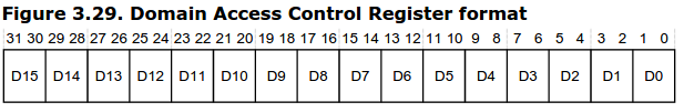
- Setup Domain Access Control Register
- Domain:
支援16個domain,一個domain包含若干個sections。Domain可被設定成 (DACR,
Domain Access Control Register):
- No access (0b00): 只要存取該記憶體空間,則觸發Domain fault。
- Clients (0x01): 做存取權限檢查,也就是有可能產生Permission fault。
- Managers (0x11): 不做存取權限檢查,不會產生Permission fault。
.. code-block:: ARM assembly
LDR     r0, 0x55555555
MCR     p15, #0, r0, c3, c0, #0
- Setup Translation Table(設定TTBR0/TTBR1)
.. code-block:: ARM assembly
MCR p15, #0, r0, c2, c0, #0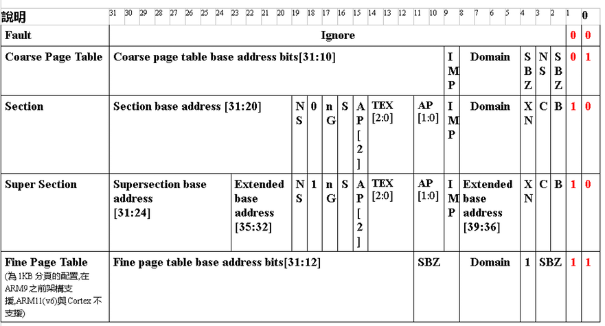
- C : Cacheable
- B : Buferrable
- TEX[2:0] : TEX Type Extension (TEX) bit 如下以SCTLR.TRE=0 (透過CP15的c1取得 System Control Register 32bits值的bit 28 來設定),也就是TEX Remap disabled模式,來說明記憶體區段屬性的配置與意義.
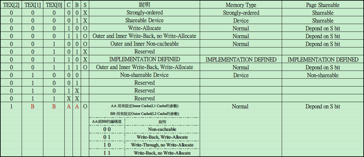
XN : 為Execute Never 的屬性,若該記憶體分頁 XN Bit設定為1,表示該分頁不會被處理器Fetch指令進來執行,在Client Domain (也就是會稽核Access Permission狀態)下,記憶體分頁必須要 XN Bit為0,且記憶體屬性是設定為可讀取,同時沒有其他Prefech Abort發生的狀態下,才可以被執行. 如果該記憶體分頁是屬於Manager Domain,XN Bit就不會被當做稽核的條件. (所以就可以嘗試去執行,而不會導致例外發生).
NS : 這個屬性在支援 Trust Zone Security Extensions環境下,才會有作用.
Domain : 參考ARMv7的文件, VMSA() 會以4-bits表示Domain的Index,也就是說最大可以定義到16個Domain,每個Domain Index會依序對應到Domain Access Control Register 32-bits值中以各2-bits依序產生的16個欄位.
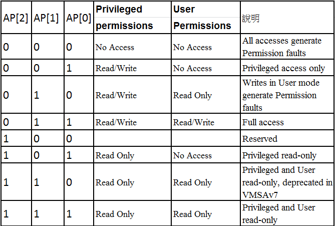
AP[2:0] :
S : 用以定義該記憶體分頁是否為Shareable,S為 0 表示該記憶體分頁為Non-shareable,S 為 1 表示該記憶體分頁為 Shareable.
nG : 這屬性為Non-Global,用來定義該記憶體分頁是否為Global,如果nG為0,表示該記憶體分頁為Global,如果為1,表示該記憶體分頁屬於目前正在運作的ASID(Address Space Identifier),該值會對應到正在運作的Task (請參考CONTEXTIDR)
Bit [18] : when bits [1:0] == 0b10
- 0 Descriptor is for a Section.
- 1 Descriptor is for a Supersection.
- Enable MMU
.. code-block:: ARM assembly
MRC     p15, #0, r0, c1, c0, #0
ORR     r0, r0, #0x001
MCR     p15, #0, r0, c1, c0, #0    ; Set MMU Enable bit
- Enable Instruction Cache
.. code-block:: ARM assembly
MRC     p15, #0, r0, c1, c0, #0
ORR     r0,  r0, #0x00001000
MCR     p15, #0, r0, c1, c0, #0
- Enable Data Cache
.. code-block:: ARM assembly
MRC     p15, #0, r0, c1, c0, #0
ORR     r0,  r0, #0x00000004
MCR     p15, #0, r0, c1, c0, #0
DEMO
TTBR0的參數定義
.. code-block:: C
#define DESC_SEC        (0x2)
#define AP_RW           (3<<10) //supervisor=RW, user=RW
#define CB              (3<<2)  //cache_on, write_back
#define NCNB            (0<<2)  //cache_off,WR_BUF off
#define DOMAIN0         (0x0<<5)
#define RW_NCNB         (AP_RW|DOMAIN0|NCNB|DESC_SEC)   /* Read/Write without cache and write buffer */
#define RW_CB           (AP_RW|DOMAIN0|CB|DESC_SEC)     /* Read/Write, cache, write back */
#define DESC_ONE        (0x1)
#define DOMAIN1         (0x1<<5)
#define ATTR_INNER      (DESC_ONE | DOMAIN1)
#define RW_FA           ((0<<9)|(3<<4)) //AP[2] | AP[1:0], read/write full access
#define WB_WA           (7 << 6) //TEX ,write back ,write allocate
#define S               (1<<10) //sharable
#define nG              (1<<11) // non global
#define ATTR_OUTER      (DESC_SEC | RW_FA | WB_WA | S | nG
設定TTBR0
.. code-block:: C
void mmu_setmtt(unsigned int vaddrStart, unsigned int vaddrEnd, unsigned int paddrStart, unsigned int attr)
{
    volatile unsigned int *pTT;
    volatile int i,nSec;
    pTT=(unsigned int *)_page_table+(vaddrStart>>20);
    nSec=(vaddrEnd>>20)-(vaddrStart>>20);
    for(i=0;i<=nSec;i++)
    {
        *pTT = attr |(((paddrStart>>20)+i)<<20);
        pTT++;
    }
}
設定 Page Table(Small page)
.. code-block:: C
//set Small Page Table
void mmu_setpg(unsigned int vaddrStart,unsigned int pageTableBassAddress, unsigned int paddrStart)
{
    volatile unsigned int *pTT;
    volatile unsigned int *pTT2;
    volatile int j;
    pTT=(unsigned int *)_page_table+(vaddrStart>>20);
    pTT2=(unsigned int *)pageTableBassAddress;
    *pTT = ATTR_INNER | ((pageTableBassAddress>>10)<<10);

    for(j =0; j < 256 ; j++){
        *pTT2 = ATTR_OUTER | (((paddrStart>>12)+j)<<12);
        pTT2++;
    }
}
.. code-block:: C
/* set page table */
mmu_setmtt(0x00000000, 0xFFFFFFFF, 0x00000000, RW_NCNB); /* None cached for 4G memory */
mmu_setmtt(0x90000000, 0xB0000000-1, 0xA0600000, RW_CB); /* cached DDR Memory */
mmu_setmtt(0xB0000000, 0xD8000000-1, 0xA0600000, RW_NCNB); /* none-cached DDR memory */
mmu_setmtt(0x80000000, 0x80020000-1, 0x80000000, RW_CB); /* 128k OnChip memory */
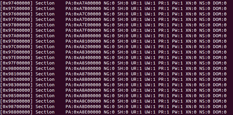
mmu_setpg(0x90000000,0xA0600000,0xC0000000); /* (VA,section address, PA) */記憶體映射位址對照
問題討論
Q1: Cortex A8 pipeline整數運算有幾級
13-stage integer pipeline
source : http://processors.wiki.ti.com/index.php/Cortex-A8_Architecture
Q2: five stage 為什麼有WB?
During this stage, both single cycle and two cycle instructions write their results into the register file.
Q3: 什麼是spinlock hazard?
The longer a lock is held by a thread, the greater the risk is that the thread will be interrupted by the OS scheduler while holding the lock. If this happens, other threads will be left “spinning” (repeatedly trying to acquire the lock), while the thread holding the lock is not making progress towards releasing it.
Q4: Beaglebone black 有幾種開機方法?
http://processors.wiki.ti.com/index.php/AM335X_StarterWare_Booting_And_Flashing
- 1.6.1 Stages in SPI Booting
- 1.6.2 Stages in NAND Booting
- 1.6.3 Stages in SD Booting
- 1.6.4 Stages in UART Booting
Q5: eMMC在板子的哪裡?
Q6: ROM code 的功能與限制?
ROM Code主要有幾項任務: * Stack Setup * Watchdog timer 1 configuration (set to three minutes) * System clock configuration * Search bootable devices (must be the FAT 12/16/32 partition) for a valid booting image (the image name must be MLO) * Load the content of the file “MLO” from a bootable device to internal RAM (the 128KB on-chip memory) * Execute the file “MLO” stored in internal RAM
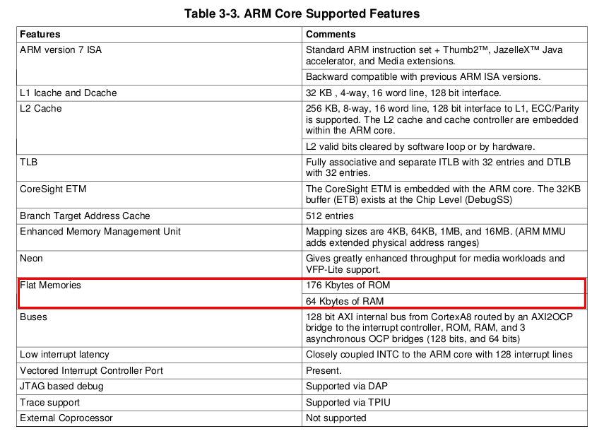
ROM code可放的容量很小,在am335x technical reference manual中提到cortex-a8的ROM code只有176kbyte(下表),因此能做的事不多
Q7: 什麼是 TCM(Tightly-Coupled Memory)?
TCM 是一個固定大小的RAM,緊密地耦合至處理器內核,提供與cache相當的性能,相較於cache的優點是,程式碼可以精確地控制什麼函數或代碼放在 RAM的哪裡。TCM對於以下幾種情況的代碼是非常有用、也是需要的:predictable及時處理(中斷處理)、時間可預見(加密算法)、避免 cache分析(加密算法)、或者只是要求高性能的代碼(編解碼功能)。reference
Q8:為什麼fcse可以加快context switch速度? 又 ARMv6 後捨棄 FCSE,採用什麼架構?
因為不同的PID可以讓對應到相同記憶體空間的位址變成不一樣的記憶體空間,不用每次存取相同記憶體時還需要flush掉cache而增加額外負擔。 -> FCSEIDR
Q9: MIDR (Main ID Register)、CTR (Cache Type Register)、TCMTR (TCM Type Register) 是什麼?
MIDR: The purpose of the Main ID Register is to return the device ID code that contains information about the processor.
ex: To access the Main ID Register, read CP15 with:
.. code-block:: ARM assembly
MRC p15, 0, <Rd>, c0, c0, 0 ; Read Main ID RegisterCTR:The purpose of the Cache Type Register is to determine the instruction and data cache minimum line length in bytes to enable a range of addresses to be invalidated.
ex: To access the Cache Type Register, read CP15 with:
.. code-block:: ARM assembly
MRC p15, 0, <Rd>, c0, c0, 1 ; Read Cache Type RegisterTCMTR:The TCM(Tightly-coupled memory) is designed to provide low-latency memory that can be used by the processor without the unpredictability that is a feature of caches.而在Cortex-A8並沒有實作TCM
Q10: 為何不能直接改register(為什麼要先讀再寫)?
為了保留除須更改的bit(s)以外的其他設定
參考資料
- StarterWare Getting Started 02.00.XX.XX
- 嵌入式Linux学习笔记(四)-内存管理单元mmu
- arm - 韋任的維基百科
- ARM 学习笔记(四) 快速上下文切换(FCSE)技术
- ARM中MMU地址转换理解
- 3.2.71. c13, FCSE PID Register
- ARM Architecture
- ARM Processor MMU
- Memory Management: Paging
- Cortex-A8 Architecture
- ARM與Cortex筆記-ARM MPCore (Multi-Processor Core) 多核心架構解析
- 有關 Cache 的 read/write through/back/allocate 的意義
